
The AI Revolution in PCB Design
AI is transforming PCB design workflows. Major EDA platforms and tool-agnostic automation providers now offer schematic verification, auto-placement, and intelligent routing features. But here's the question most engineers overlook: How does AI actually read your schematic?
Your schematic isn't just a visual diagram for humans—it's data for machines. Whether you're using Altium, Cadence, or KiCad, the way you structure your schematic directly impacts how well AI tools can understand your design intent.
What Makes a Schematic "AI-Ready"?
AI platforms need structured, machine-readable data to provide meaningful automation. This means:
- Consistent naming conventions that algorithms can parse
- Complete metadata (component specs, lifecycle, suppliers)
- Clear hierarchy and signal flow documentation
- Standardized formats that preserve design context
This guide shows you how to design schematics that both humans and AI systems can understand—enabling better automation, faster reviews, and fewer layout errors.
1. What a schematic is and why structure matters
A PCB schematic is the main reference for your circuit. It shows all the parts (symbols), how they connect (nets), and what each part does (labels and notes). It’s readable by both humans and design tools.
A well-structured schematic makes your work faster, clearer, and more reliable.
- Components: Each part in the circuit—like resistors, capacitors, transistors, ICs, and connectors—is represented by a symbol.
- Connections (Nets): Lines connect the symbols to show how current and signals flow.
- Labels: Names for important signals, such as VCC, GND, or RESET.
- Notes: Describe values or part details for better understanding and documentation.
In short, a schematic is the blueprint of your circuit’s logic, showing what connects to what and how the circuit is meant to function—before it’s turned into a physical PCB.
⚠️ AI Impact if not followed:
Without proper structure and clear component representation, AI tools cannot accurately parse the circuit's logic or identify relationships between components. This leads to failed design intent recognition, incorrect connectivity analysis, and unreliable automated verification results. AI agents really likes good resolution images, and unnecessary clutter can confuse the engine.
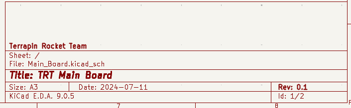
2. Page / frame hygiene: title block, revision history, ToC
Include a title block on every sheet with project/sheet info, author/owner, contact, and a machine‑parseable revision history. Add a table of contents and cross‑sheet numbering for multi‑sheet designs.
- Project title, sheet name/number (e.g.,
Sheet 2 / Power), and total sheet count. - Author/owner/company/contact, and an ISO date for version control
- Revision history (who/when/why) and doc comments/explanatory notes.
- Cross‑references (to sheets, to nets) and consistent hierarchy tags.
⚠️ AI Impact if not followed:
Missing or inconsistent title blocks and revision history prevent AI tools from tracking design versions, understanding project context, and maintaining proper documentation lineage. Automated tools cannot reliably identify sheet relationships or cross-reference connections without standardized metadata.
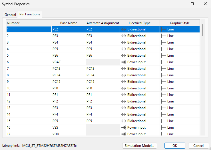
3. Symbols & Libraries
Use clear, standardized schematic symbols and make sure each symbol connects correctly to its footprint. Always check polarity, pin numbers, and multi-unit parts (like U1A/U1B) for accuracy.
- Pin Mapping: Match symbol pins to footprint pins clearly—no guessing or swapped connections.
- Polarity & Orientation: Show pin 1, notches, or polarity marks on the symbol and footprint.
- Footprint Link: Reference a verified footprint
- Component Data: Keep key fields like value, rating, package, and part number complete and consistent.
- Lifecycle Tracking: Note whether parts are active, obsolete, or under review.
⚠️ AI Impact if not followed:
Non-standard symbols or incorrect symbol-to-footprint mappings confuse AI parsers, leading to misidentified components and incorrect pin assignments. This results in failed ERC checks and potentially dangerous errors in the final PCB layout.
4. Good Metadata & Library Context
Rich, consistent metadata and a clean, verified library are the backbone of a professional schematic. They make your design traceable, machine-readable, and ready for AI-assisted workflows.
Why Metadata Matters
Metadata turns your schematic from a visual diagram into a data-rich source of truth. It enables tools to understand not just what you connected, but why and how those components behave in the system.
- Traceability: Each component, net, and sheet can be tracked through manufacturing and maintenance.
- Data integrity: Reduces manual entry errors and ensures consistent attributes across revisions.
Essential Metadata Fields
- Manufacturer Part Number (MPN) – Enables direct sourcing and price tracking.
- Manufacturer Name – Ensures accurate reference for lifecycle and datasheet verification.
- Package / Footprint – Matches schematic symbol to physical PCB layout.
- Electrical Attributes – Voltage, current, power, tolerance, and frequency ranges.
- Lifecycle Status – Active, NRND (Not Recommended for New Design), or Obsolete.
- Supplier & Distributor IDs – LCSC, DigiKey, Mouser, or Arrow identifiers.
- Revision Tags – Version control tags that sync with Git or PLM systems.
Library Management Best Practices
- Centralized Library: Maintain a single source for schematic symbols, footprints, and 3D models.
- Validation Scripts: Pin-mapping checks to flag mismatches across board files and schematic.
- Parameter Templates: Define a shared metadata schema to ensure consistent field names.
⚠️ AI Impact if not followed:
Incomplete or missing component metadata (MPN, manufacturer, lifecycle status) prevents AI tools from performing accurate BOM validation, sourcing analysis, and lifecycle management.
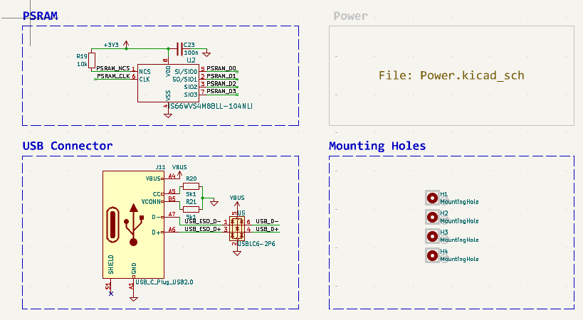
5. Small, Structured & Neatly Arranged Content
Neat schematic organization makes your design easier to read, verify, and modify. Every symbol, wire, and label should have a clear purpose and logical placement.
- Compact layout: Keep related components close together in small logical blocks (e.g., power section, MCU I/O, sensors).
- Alignment & spacing: Align symbols to the schematic grid and maintain consistent spacing between elements.
- Readable signal flow: Arrange the circuit so that signals flow from left to right and power flows top to bottom.
- Labels over wires: Use net labels instead of long, crossing wires to keep diagrams clean and minimal.
- Annotations & notes: Add small, structured comments near functional groups for quick understanding.
- Grouping & borders: Use rectangles or dashed outlines to visually group subsystems for easier debugging and documentation.
- Whitespace balance: Don’t overcrowd. Leave breathing room between nets and components to improve readability.
⚠️ AI Impact if not followed:
Cluttered, poorly organized schematics with overlapping symbols or unclear signal flow make it nearly impossible for AI algorithms to accurately trace connections and understand circuit topology.
6. Smart & Consistent Net Naming: How to Keep Your Schematic Organized
Net naming is the language your schematic uses to communicate both with engineers and design tools. A clear, systematic naming convention eliminates confusion, speeds up debugging, and ensures smooth integration between schematic, PCB layout, and firmware development. Whether you're handling simple GPIOs or complex high-speed interfaces, meaningful names make collaboration and automation far easier.
Core Principles of Good Net Naming
- Be descriptive but concise: Use names that describe purpose and behavior — e.g.,
MCU_RESET_N,3V3_IO,USB_DP. - Show hierarchy or ownership: Prefix nets by subsystem or device, such as
MCU_,SENSOR_,POWER_, orCOMM_. - Follow active-low convention: Append
_Nor_Bfor active-low signals (e.g.,RESET_N). - Keep syntax tool-safe: Avoid spaces, slashes, or symbols; use underscores (
_) and consistent capitalization. - Maintain consistency: Use the same naming scheme across all schematic sheets, libraries, and PCB netlists.
Signal-Level Net Naming
For GPIOs, peripheral interfaces, and control signals, clarity is critical. Signal nets should tell you what device drives them, what function they serve, and their direction or type.
- GPIOs: Name based on function, not just pin number. For example:
GPIO_LED1— General-purpose output driving LED1.GPIO_BTN_IN— Input connected to a user button.GPIO_FAN_EN— Output enabling fan control.
- Peripheral interfaces: Use protocol-specific prefixes for clarity:
UART_TX,UART_RX— UART transmit/receive lines.SPI_MOSI,SPI_MISO,SPI_SCK,SPI_CS— SPI interface signals.I2C_SDA,I2C_SCL— I²C communication lines.CAN_H,CAN_L— CAN bus differential pair.ETH_TX_P,ETH_TX_N— Ethernet differential pairs for transmit lines.
- Control signals: Name based on their intent or logical function, e.g.:
PWR_EN— Power enable line.CHG_STAT— Charger status signal.SENSOR_ALERT— Interrupt output from a sensor.SYS_READY— Indicates system initialization complete.
- Analog & feedback nets: For measurement or feedback signals, include their reference, such as:
V_SENSE,CURRENT_FB,TEMP_MON.
- Differential pairs: Always suffix with
_Pand_N, likeUSB_DP/USB_DNorLVDS_CLK_P/LVDS_CLK_N.
Power Domains & Special Nets
- Voltage rails: Specify voltage and purpose —
1V2_CORE,3V3_IO,5V_USB,VBAT. - Grounds: Distinguish different domains —
AGND(analog),DGND(digital),PGND(power). - Isolated / switched nets: Use
_ISOor_SWfor clarity (e.g.,5V_SWfor switched 5V).
Common Net Naming Examples
| Category | Example | Description |
|---|---|---|
| Power Rails | 3V3_IO, 1V2_CORE |
Indicates voltage level and usage domain. |
| Differential Pairs | USB_DP, USB_DN |
Paired nets for high-speed signaling (differential). |
| Control Signals | RESET_N, PWR_EN |
Logic control lines; use “_N” for active-low. |
| GPIO / Digital I/O | GPIO_LED1, GPIO_BTN_IN, MCU_GPIO23 |
General-purpose I/O lines, named by function or controller pin. |
| Communication Buses | UART_TX, SPI_MISO, I2C_SDA, CAN_L |
Standard protocol lines for external communication. |
| Analog / Sensor Signals | V_SENSE, TEMP_MON, CURR_FB |
Analog feedback or measurement nodes. |
⚠️ AI Impact if not followed:
Inconsistent or ambiguous net naming prevents AI tools from correctly identifying signal types, power domains, and differential pairs.
7. Reference Designators: Table & Cheat-Sheet
Use standard IEEE-style prefixes (R, C, U, J, L, TP, etc.). Each designator should be unique and remain consistent across schematic revisions to avoid confusion.
Common Reference Designators
| Component Type | Prefix | Example |
|---|---|---|
| Resistor | R | R1, R10 |
| Capacitor | C | C1, C22 |
| Inductor | L | L1, L5 |
| Diode | D | D1, D2 |
| Transistor / MOSFET | Q | Q1, Q3 |
| Integrated Circuit (IC) | U | U1, U2A (multi-unit) |
| Connector | J | J1, J2 |
| Test Point | TP | TP1, TP_GND |
| Fuse | F | F1, F2 |
| Switch / Button | S | S1, S2 |
| LED | LED | LED1, LED2 |
| Crystal / Oscillator | Y | Y1, Y2 |
| Ferrite Bead | FB | FB1, FB2 |
| Mechanical Part / Mounting Hole | M | M1, M2 |
⚠️ AI Impact if not followed:
Inconsistent or duplicate reference designators cause AI parsers to fail in component identification and BOM generation.
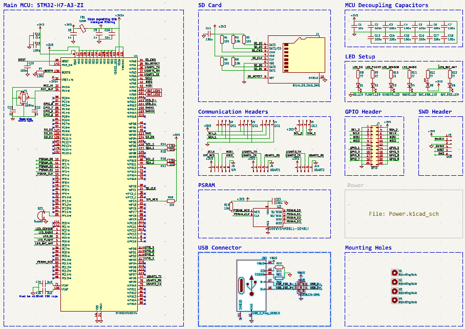
8. Schematic Sub-Sectioning & Title Blocks
Breaking your schematic into well-defined, titled sections makes complex designs easier to navigate and maintain. Each section should represent a logical function of your circuit, with a clear title block and standardized layout. This structure improves readability, supports team collaboration, and allows automated tools (ERC/DRC or AI parsers) to analyze your design accurately.
Why Sub-Sectioning Matters
- Clarity: Organized schematic sheets help new engineers or reviewers quickly locate specific circuit blocks.
- Scalability: Modular sections make it easy to reuse functional blocks in future projects.
- Automation-Friendly: Hierarchical titles and metadata fields help scripts identify related nets, power domains, and subsystems automatically.
- Documentation: Each block becomes self-descriptive with its title, revision, and responsible author noted directly on the sheet.
Typical Schematic Sub-Sections
| Section Name | Description | Typical Components |
|---|---|---|
| Power Input & Regulation | Defines how the board receives and converts power. Should include voltage regulators, protection circuits, and power nets (e.g., +5V, +3V3, 1V2_CORE). | DC jacks, fuses, diodes, LDOs, DC-DC converters, bulk capacitors. |
| Microcontroller / Processor Core | Contains the main MCU, its decoupling, reset, clock, and configuration circuitry. | MCU/CPU, crystals, capacitors, resistors, programming connectors. |
| Memory & Storage | Interfaces for Flash, EEPROM, or RAM connected to the core logic. Group near related buses. | SPI flash, SDRAM, EEPROM, memory sockets. |
| Sensors & Analog Inputs | Sensor signal conditioning and analog measurement circuits. Include isolation and filtering if needed. | Op-amps, ADCs, resistors, capacitors, connectors. |
| Communication Interfaces | External communication ports such as USB, UART, I2C, SPI, or CAN. Group by voltage domain and shielding. | Connectors, level shifters, ESD diodes, filters. |
| Clock & Timing | Provides oscillators, crystals, and timing references for synchronous systems. | Crystals, oscillators, load capacitors, resistors. |
| Test & Debug | Dedicated area for measurement, in-circuit test, and programming headers. | Test points, JTAG/SWD connectors, debug LEDs. |
| Mechanical & Interface Elements | Mounting holes, alignment marks, or mechanical connectors placed for PCB integration. | Mounting pads, connectors, board edges, fiducials. |
Title Block & Metadata Fields
Each schematic sheet should include a title block containing structured metadata fields. This ensures consistent documentation across all design sheets.
- Project Name / Code: Unique identifier for the entire design (e.g., “PWR-CTRL-V3”).
- Sheet Title: Functional area title (e.g., “MCU Core & Reset Logic”).
- Sheet Number: (e.g., Sheet 3 of 10) for multi-page designs.
- Author / Reviewer: Designer and reviewer names with revision date.
- Version / Revision: Numeric or semantic version (e.g., Rev. A1, v2.3.0).
- Change History: Small revision log summarizing edits and responsible engineer.
- Cross-References: Pointers to related sheets or subsystems (e.g., “See Sheet 4: Power Distribution”).
⚠️ AI Impact if not followed:
Without logical sub-sectioning and clear hierarchy, AI tools cannot understand functional blocks or module relationships. This prevents effective design reuse, modular verification, and intelligent component grouping for layout optimization.
9. FAQ
How does AI use schematic designs?
Our algorithms analyze schematics to understand design intent, detect logical relationships, and verify connectivity or compliance. They interpret the net naming and component metadata to identify how each block functions in the system. Additionally, many companies are now using AI for schematic verification to automate design review processes and ensure compliance with engineering standards. Beyond that, AI tools are used for:
- Design validation: Checking ERC/DRC consistency, missing connections, or polarity errors.
- Debugging: Detecting mislabeled nets, overlapping symbols, or wrong footprints.
- Parsing & indexing: Creating a machine-readable graph of components and nets for reuse or documentation.
- Learning patterns: Comparing new designs to known templates or industry standards.
Which Circuit Design AI algorithms are used for schematic processing?
Modern schematic analysis uses a mix of algorithms, including large language models (LLMs) for context understanding and graph-based parsers for net connectivity and symbol interpretation. However, online LLMs can pose data privacy risks if designs are processed externally. That’s why we emphasize secure, offline AI parsers that operate entirely on your local system or private network.
Our approach is built on on-premise, sandboxed processing — no cloud upload, no external data mining. This protects your IP and ensures schematic data stays confidential. In summary:
- ✅ Offline parsing = no data leakage, fully local.
- ✅ Secure design analysis = runs on your own machine.
- ⚠️ Cloud-based AI may offer convenience, but carries IP and compliance risks.
What’s the impact of a bad schematic (or ignoring best practices)?
Ignoring schematic organization and metadata standards affects both human readability and AI readability. A poorly structured schematic with inconsistent net names, missing component data, or messy layout leads to:
- ❌ Confusing documentation and slow debugging.
- ❌ Failed ERC/DRC or incorrect BOM outputs.
- ❌ Misinterpreted nets and incomplete exports.
- ❌ Broken AI parsing or rule-based checks.
Good schematic readability = good AI readability. The same clarity that helps engineers understand your design helps automated systems process it correctly. Structured naming, hierarchy, and complete metadata make your schematic both machine-ready and review-friendly.
Should I export a schematic as JSON or XML for AI tools?
No need, most AI tools can read the existing design files directly without requiring export to JSON or XML formats.
What's the right way to name differential pairs for PCIe, USB, or Ethernet?
Use _P / _N suffix for differential pair naming (e.g., USB_DP, USB_DN). Additionally, add impedance and length matching rules in the net class to ensure signal integrity.
10. Design readiness checklist (BOM + connectivity)
Make your schematic manufacturing-ready and machine-readable. Tick each item as you complete it. Your progress is saved locally in this browser. For PCB design checklist refer the PCB design checklist.
General Design Review
Component Selection
Power Supply Design
Signal Integrity
Interface Connections
Reset and Clock Circuits
Programming/Debug Interfaces
Component Connections
Designators and Values
Net Names and Labels
Protection Circuits
Test Points
Documentation
Electrical Rules Check (ERC)
Design for Manufacturing (DFM)
High-Speed Digital Design
Impedance and Transmission Lines
Termination Schemes
Clock Distribution
High-Speed Interfaces
Signal Integrity Considerations
Power Integrity for High-Speed
EMI/EMC Considerations
Timing Analysis
Turn Your Schematic into a Real PCB
You’ve designed a clean, structured schematic — now it’s time to bring it to life. Convert your schematic into a fabrication-ready PCB using industry-standard workflows. Whether you’re working in KiCad, Altium Designer, Cadence or another tool, our step-by-step resources help you go from design intent to a manufacturable board — fast.
Contact Us