
TL;DR — 15 Takeaways
- 90° corners — Negligible impact on most digital nets. Use 45°/arcs only on impedance-controlled and RF traces.
- Serpentine tuning — Match topology first; meander only the remaining skew with ≥ 3 W segment spacing.
- 50 Ω everywhere — Match impedance to the interface spec: USB2 = 90 Ω, PCIe/USB3 = 85 Ω, Ethernet = 100 Ω. Many nets need no impedance control at all.
- Clock frequency ≠ speed — Rise time determines bandwidth. A 10 MHz clock with a 1 ns edge is a 350 MHz problem.
- Termination at low frequencies — Fast edges + long traces ring regardless of clock rate. Evaluate by edge rate, not frequency.
- Ground plane splits — Both "always split" and "never split" are wrong. Design the return-current loop.
- Copper pour everywhere — Unstitched islands radiate; narrow slots act as antennas. Pour deliberately, stitch regularly.
- Guard traces — Only work when stitched to the reference plane at close intervals. Increasing spacing is often simpler and more effective.
- Diff pair return path is the other trace — On PCB, the reference plane still carries the majority of the return current. Always provide a continuous plane.
- Three-decade decap rule — Can create anti-resonance peaks. Follow the IC vendor's recommendations and minimize mounting inductance.
- Cap placement is everything — On tightly coupled plane pairs, via loop inductance matters more than an extra millimeter of distance.
- More ferrites = less noise — Can worsen noise through LC resonance. Address loop area and return paths first.
- All via stubs are bad — Calculate stub resonance vs. signal bandwidth. Standard 1.6 mm boards are fine for most sub-GHz signals.
- Working prototype = good design — "It works" means one sample passed one condition. Measure margin for production confidence.
- Always use thermal relief — Default yes, but remove on high-current pads, thermal pads, and low-inductance ground connections.
Quick Navigation
PCB design is full of rules passed from engineer to engineer, often without the context that made them rules in the first place. Some originated in 1980s fabrication processes. Others were true for specific technologies but got generalized beyond recognition. A few were never quite right.
This is not a list of "wrong" rules. Most exist for real reasons. The problem is applying them as absolutes — when the answer should almost always be "it depends on your design."
Each entry below covers: why the rule exists, when it genuinely applies, when it doesn't, and what to think about instead.
Routing Geometry
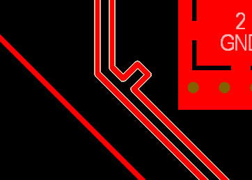
1. "Never route 90° corners."
This rule traces back to two real concerns. The first is etching defects: in older subtractive processes, acute internal angles (sharper than 90°) could trap etchant and cause over-etching. Right angles themselves are less prone to acid trapping than acute corners, but the fear was generalized. Modern photolithographic processes with controlled spray etching have largely eliminated this as a practical failure mode on standard geometries.
The second concern is electrical. A 90° bend creates a small capacitive discontinuity because the effective trace width increases at the outer corner. This extra copper adds capacitance to ground, which locally changes the impedance. How much this matters depends entirely on how large that corner geometry is relative to the signal's edge-rate wavelength.
At typical digital speeds — even at a few hundred MHz — the corner discontinuity is electrically tiny. The added capacitance from a standard 90° corner on a 5-mil trace is on the order of a few femtofarads. A standard through-hole via introduces significantly more parasitic capacitance than a right-angle bend.
When 90° corners are fine: Low-speed digital signals (GPIO, I²C, UART, SPI at moderate rates), power distribution traces, dense routing where space is constrained, and any net where impedance control is not required.
When to use 45° or arcs instead: Controlled-impedance lines (USB, DDR, PCIe, HDMI), RF traces where the corner geometry approaches a meaningful fraction of the edge-rate wavelength, and high-voltage traces where field concentration at sharp corners affects creepage/clearance margins.
The Better Rule
Don't fear 90° corners universally. Fear uncontrolled impedance changes on critical nets. For the majority of traces on a typical embedded board, the corner angle has negligible electrical impact. For impedance-controlled and RF nets, use 45° mitred bends or arcs — not because of a blanket rule, but because you're managing a specific impedance discontinuity on a specific net class.
Reference: Bogatin, E. "Signal and Power Integrity — Simplified," Chapter on transmission line discontinuities. Also see Johnson, H. & Graham, M. "High-Speed Digital Design" for quantitative analysis of right-angle bend capacitance.
2. "Serpentine length tuning is harmless — add it wherever needed."
Length tuning with serpentine (meander) patterns is a legitimate technique for matching propagation delay between traces, particularly in parallel buses and differential pairs. The problem is when it's applied reflexively without considering what it introduces.
Every serpentine section creates parallel trace segments in close proximity. These segments couple to each other electromagnetically. If the meander segments are too close or too long, this coupling creates crosstalk between adjacent meander segments, localized impedance changes where the effective geometry deviates from a clean transmission line, and potential mode conversion in differential pairs if only one trace is meandered.
In differential pairs, the practical recommendation is to first match path topology and via count between the P and N traces. If the remaining skew is small, gentle meanders with adequate spacing between segments (at least 3× the trace width) handle the rest. Aggressive serpentines with tight spacing introduce more problems than the original skew.
When tuning is required: Parallel buses with tight setup/hold timing (DDR memory interfaces), differential pairs where the protocol defines a specific intra-pair skew budget (USB 3.x, PCIe), and clock distribution networks requiring matched delays.
When tuning creates problems: Over-matching differential pairs beyond what the protocol spec requires, using tight meander spacing that creates self-coupling, adding serpentines on nets where the timing margin is already generous, and meandering only one leg of a differential pair (this converts differential mode energy to common mode, increasing EMI).
The Better Rule
Length-tune only to what the protocol timing budget requires. Match topology first — same number of vias, same layer transitions, same path structure. Then add gentle meanders with ≥ 3 W spacing between segments for the remaining mismatch. USB 2.0 HS allows roughly 100 ps of intra-pair skew, which is usually easy to meet on a PCB without aggressive serpentines. Check your protocol spec before over-constraining.

3. "Everything must be 50 Ω."
50 Ω is the standard impedance for most test equipment, coaxial cables, and many RF systems. It's a historical engineering compromise: 50 Ω falls between the impedance that minimizes loss in air-dielectric coax (approximately 77 Ω) and the impedance that maximizes power handling (approximately 30 Ω). The RF and test-equipment world standardized on 50 Ω, and it became the default assumption.
But many interfaces on a PCB don't use 50 Ω. Common differential impedance targets include:
| Interface | Typical Differential Impedance | Notes |
|---|---|---|
| USB 2.0 (HS) | 90 Ω ±15% | Per USB 2.0 specification |
| USB 3.x (SuperSpeed) | 85 Ω ±15% | Check your PHY vendor's guide; some references cite 90 Ω |
| PCIe (CEM/add-in card) | 85 Ω | PCI-SIG CEM spec; on-board may differ |
| 1000BASE-T Ethernet | 100 Ω ±15% | IEEE 802.3 |
| LVDS | 100 Ω | ANSI/TIA/EIA-644 |
| CAN Bus | 120 Ω (single-ended bus impedance) | ISO 11898 |
Not every trace on a board requires controlled impedance at all. A GPIO running at 10 MHz over a 2 cm trace doesn't need impedance control. Applying 50 Ω geometry to every net wastes board space and can complicate routing.
What determines whether a net needs impedance control: The relationship between trace length and the signal's rise time. If the trace length exceeds roughly one-sixth of the electrical length of the rising edge, treat it as a transmission line and control the impedance. Below that threshold, impedance control provides little benefit.
The Better Rule
Match impedance to the interface specification, not to a default number. Identify which nets actually require controlled impedance based on edge rate and trace length. Define impedance targets per net class in your design rules, derived from your stackup and the protocol requirements. 50 Ω is correct for some nets, wrong for others, and unnecessary for many.
Reference: PCI-SIG CEM specification for PCIe impedance targets. USB-IF specifications for USB 2.0 / 3.x impedance. IEEE 802.3 for Ethernet. Pozar, D. "Microwave Engineering" for the historical 50 Ω compromise derivation.
What Counts as "High-Speed"
4. "Clock frequency tells you if a signal is high-speed."
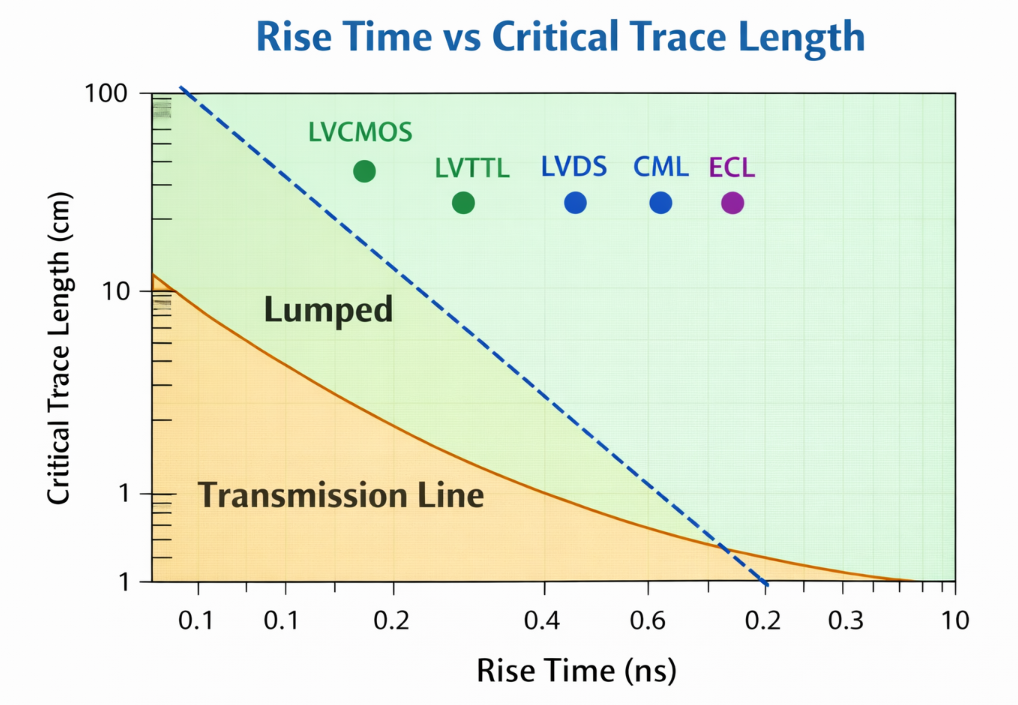
This is probably the single most consequential misunderstanding in PCB design. The frequency of a periodic signal tells you its repetition rate. It does not tell you how fast the voltage transitions between states. That's the rise time (or fall time), and it's what determines the signal's actual bandwidth — the range of frequencies present in the signal that the PCB must faithfully transmit.
A 10 MHz square clock with 1 ns rise time contains significant spectral energy up to approximately 350 MHz. This comes from the commonly used one-pole approximation BW ≈ 0.35 / trise. That means a 10 MHz signal can require the same PCB treatment as a 350 MHz sine wave in terms of impedance control and return path management.
Example: 1 ns rise time → BW ≈ 350 MHz
Example: 200 ps rise time → BW ≈ 1.75 GHz
Modern CMOS drivers often have rise times well under 1 ns, regardless of clock frequency. A microcontroller GPIO configured as a 25 MHz output may have a 500 ps edge, putting its bandwidth content above 700 MHz. The PCB responds to the edge, not the clock.
This determines when you need transmission-line treatment. A common rule of thumb: if the one-way propagation delay of a trace exceeds about one-sixth of the signal's rise time, reflections from impedance mismatches become significant and the trace should be treated as a transmission line. (Different references use different thresholds — one-sixth to one-tenth — depending on how much reflection is acceptable. One-sixth is a common moderate threshold.)
On FR-4, signals propagate at roughly 6 inches (15 cm) per nanosecond for outer-layer microstrip (the exact value depends on the effective dielectric constant of your stackup — typically 3.0 to 3.8 for microstrip). For a 1 ns rise time using the one-sixth threshold, the critical length is approximately 1 inch (2.5 cm).
The Better Rule
Classify signals by rise time and trace length, not clock frequency. Check the driver's datasheet for edge rate specifications. If the propagation delay of the trace exceeds ~trise/6, treat the net as a transmission line. A "slow" 20 MHz clock with a fast driver may need more care than you expect.
Reference: Bogatin, E. "Signal and Power Integrity — Simplified," Chapters 2–3 on bandwidth, rise time, and critical length. Johnson, H. & Graham, M. "High-Speed Digital Design," Chapter 1.
5. "Termination isn't needed at low frequencies."
This follows directly from the frequency misconception above. A 25 MHz SPI bus sounds like it shouldn't need termination. But if the driver has a 500 ps rise time and the trace runs 10 cm, the signal will reflect off the impedance discontinuity at the receiver, travel back to the driver, and reflect again — causing ringing that can violate the receiver's input thresholds or stress its ESD protection.
With modern low-impedance CMOS drivers (often 10–30 Ω output impedance) driving a trace into a high-impedance CMOS input (effectively an open circuit at signal frequencies), the reflection coefficient at the receiver is nearly +1. Almost all signal energy reflects back. On short traces, reflections settle before the receiver samples. On long traces with fast edges, they don't.
When termination is needed: Whenever the trace is electrically long relative to the rise time and the source/load impedances are significantly mismatched. This can apply to GPIO lines, SPI clocks, reset lines — any signal with a fast driver and a long enough trace.
Common termination approaches: Series termination at the source (a resistor matching the difference between driver impedance and trace impedance) is simplest for point-to-point connections — it absorbs the reflected wave when it returns to the source. Parallel termination at the receiver is used when the receiver must see a clean waveform immediately, but it draws DC current.
The Better Rule
Evaluate termination need based on edge rate and trace length, not clock frequency. If you see ringing on a "slow" bus during bring-up, it's a reflection problem. Check the driver's output impedance and rise time in the datasheet, and compare trace length to the critical length for that edge rate.
Planes, Pours & Return Paths
6. "Always split analog and digital grounds." / "Never split ground planes."
Both absolutes fail. The real principle underneath is return current management — understanding where current actually flows and designing the copper to support that.
Why splits cause problems: When a signal trace crosses a gap in the reference plane beneath it, the return current (which flows in the plane directly under the trace at high frequencies, following the path of least inductance) must detour around the gap. This detour increases the loop area, degrades impedance control, and creates a loop antenna that radiates EMI.
Why the "always split" rule exists: In mixed-signal boards with high-resolution ADCs, digital switching currents flowing through shared ground impedance can inject noise into the analog measurement path. A split plane forces analog and digital return currents into separate copper.
Why it usually backfires: Unless every signal between the analog and digital domains crosses the split at exactly one controlled point (typically the ADC's ground pin), signals will cross the gap, forcing return currents through long, inductive detours — creating exactly the noise the split was supposed to prevent, plus EMI.
What works better for most mixed-signal designs: A single, solid ground plane with careful partitioning by placement and routing. Place analog components together, digital components together, and control where high-current digital return paths flow relative to sensitive analog traces. Follow the ADC manufacturer's datasheet for ground connection instructions at the converter.
When a split genuinely makes sense: True galvanic isolation boundaries (high-voltage safety barriers, isolated power supplies, medical-grade isolation). These are electrical isolation requirements, not noise management strategies.
The Better Rule
Design the current loop, not the copper shape. Use a solid reference plane and control where currents flow through intelligent placement and routing. If you split, know exactly which signals cross the boundary and where the return current goes. If you can't answer that for every net, the split is likely hurting more than it helps.
Reference: Ott, H. "Electromagnetic Compatibility Engineering," Chapter on grounding and mixed-signal layout. Analog Devices application note AN-1142 on mixed-signal grounding.
7. "Copper pour on signal layers always helps."
Filling empty space with copper can serve real purposes: reducing copper imbalance between layers (preventing board warpage during lamination), providing shielding, and adding thermal spreading. The problem is when "pour everywhere" becomes automatic, with no thought about connectivity or reference.
An unstitched copper island — pour that isn't connected to any net or is connected to a plane only at one distant point — can act as a resonant structure. A 3 cm copper island, for instance, has a quarter-wave resonance in the range of roughly 1–1.5 GHz on FR-4 (depending on effective dielectric constant and geometry), which is within the harmonic content of many common digital signals.
Copper pour that creates narrow slots between traces and the pour boundary also causes problems. A narrow slot in a ground pour acts as a slot antenna — an efficient radiator at frequencies related to the slot dimensions.
When pour helps: When stitched with vias to a reference plane at regular intervals, creating a well-connected extension of the reference. When it provides copper balance across layers for manufacturing. When it provides thermal spreading on power-dense areas.
When pour hurts: Floating islands with no connection or a single distant connection. Narrow slots created by pour flowing between traces. Pour on inner signal layers creating unpredictable coupling. Pour adjacent to high-speed traces where the pour edge creates an uncontrolled impedance environment.
The Better Rule
Pour deliberately, not automatically. Stitch pour to the reference plane with vias at regular intervals. Remove isolated islands that your EDA tool's DRC should flag. Check that pour doesn't create narrow slots adjacent to signal traces. A clean board with no pour is better than a board with poorly managed pour.
8. "Guard traces always reduce crosstalk."
A guard trace is a grounded trace placed between two signal traces to reduce electromagnetic coupling between them. The concept is sound — a grounded conductor shields the signals from each other. The implementation is where it fails.
For a guard trace to function as a shield, it must be connected to the reference plane at frequent intervals along its length with stitching vias. Without these vias, the guard trace is just a floating piece of copper. A floating conductor couples capacitively to both adjacent traces, and at certain frequencies, it can resonate and actually increase the coupling between them.
A guard trace grounded only at its endpoints behaves as a resonant stub at frequencies where its length corresponds to a half-wavelength. At those frequencies, the "guard" trace can amplify crosstalk rather than reduce it.
When guard traces work: When properly stitched to the reference plane with vias at close intervals. The RF-style via-fence guideline of λ/20 spacing is a useful reference, though for most digital boards the practical question is simply "stitch it frequently or don't bother." The guard must be wide enough and well-referenced enough to intercept the fringing fields between the two signal traces.
What often works better: Increasing spacing between the aggressor and victim traces. Crosstalk in microstrip falls off roughly as 1/d² (where d is edge-to-edge spacing). Doubling the spacing between two traces often provides more crosstalk reduction than adding a poorly implemented guard trace in the same footprint.
The Better Rule
If you use a guard trace, stitch it to the reference plane at regular intervals — not just at the endpoints. If you can't commit to the via stitching, increase trace spacing instead. It's simpler, more predictable, and uses less board area than a guard trace that doesn't actually guard anything.
Reference: Bogatin, E. lists guard trace effectiveness as a common myth topic in his webinar and article series. Ott, H. "Electromagnetic Compatibility Engineering" for crosstalk reduction strategies.
9. "In a differential pair, each trace is the return for the other — the reference plane is optional."
This misunderstanding comes from a partial truth. In a differential pair, the two traces carry equal and opposite currents, and a portion of the return current does flow in the complementary trace. If the traces were perfectly coupled — infinitely close together, with no other conductor nearby — all return current would flow in the partner trace and no plane would be needed.
In practice, PCB differential pairs have limited coupling. The coupling coefficient for typical PCB geometries varies significantly with trace spacing, dielectric height, and layer structure — a commonly cited range is roughly 0.2 to 0.5. The split of return current between the partner trace and the reference plane depends on this coupling, the frequency, and the geometry. The key point is that a significant portion of the return current — often the majority — flows in the reference plane, not in the partner trace.
Remove the reference plane, and you lose impedance control (differential impedance becomes unpredictable and higher than intended), field containment (fields spread out, increasing EMI), and common-mode rejection (noise induced on the pair becomes asymmetric because the field environment is no longer symmetric).
This matters in situations where differential pairs cross plane splits, route over voided areas, or transition between layers without proper stitching vias. In each case, the return current that was flowing in the plane must find an alternative path — the result is impedance discontinuity, mode conversion (differential to common mode), and EMI.
The Better Rule
Differential pairs need a continuous reference plane underneath, just like single-ended signals. The pair coupling helps with noise rejection but does not replace the plane. Route differential pairs over unbroken reference planes. When changing layers, place stitching vias near the transition to provide a return path between the old and new reference planes.
Reference: Bogatin, E. specifically identifies "the other trace is the return path" as a common myth. See "Signal and Power Integrity — Simplified," differential pair chapters. Also Ritchey, L. "Right the First Time" for practical differential routing guidance.
Decoupling & Power Integrity
10. "Always use the 0.1 µF + 1 µF + 10 µF rule at every IC."
The "three decades" rule originates from a time when ceramic capacitors had relatively poor high-frequency performance. Combining multiple values ensured useful impedance reduction across a wider frequency range.
Modern MLCCs have changed this in two ways. First, an MLCC's effective impedance depends heavily on its physical size and mounting geometry (pad design, via arrangement), not just its capacitance value. A 100 nF 0402 and a 100 nF 0805 have meaningfully different impedance curves because the package parasitics differ.
Second — the critical point — placing multiple values in parallel creates anti-resonance peaks. At the frequency between two capacitors' self-resonant frequencies, one capacitor is inductive (above its SRF) while the other is still capacitive (below its SRF). This parallel LC combination creates a resonant peak where the PDN impedance can be higher than with either capacitor alone.
What actually matters: The total mounting inductance of the capacitor — from the IC's power pin, through the trace/via to the capacitor pad, through the capacitor, and back through the return path. This loop inductance dominates the cap's effective frequency range. A 100 nF cap with 200 pH of loop inductance behaves very differently from the same cap with 1 nH.
In practice: One well-placed capacitor with a low-inductance connection often outperforms three poorly connected capacitors. Place caps close to IC power pins, use the shortest possible via connections to the planes, and choose values based on the IC vendor's recommendations — they've modeled the interaction.
The Better Rule
Choose decoupling values based on the IC's transient current requirements and your PDN target impedance, not a fixed three-decade recipe. Minimize mounting loop inductance for each cap. If the IC datasheet specifies decoupling values and placement, follow those recommendations.
Reference: Smith, L. & Bogatin, E. "Principles of Power Integrity for PDN Design — Simplified." Signal Integrity Journal articles on anti-resonance in parallel decoupling networks.
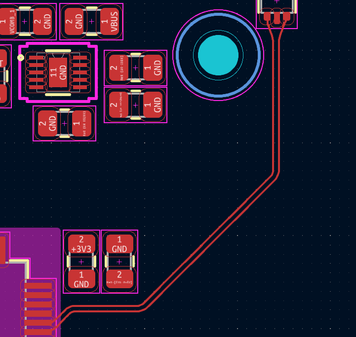
11. "Decoupling cap placement is always the most critical factor."
Placement matters — but its relative importance depends on your stackup.
When power and ground planes are closely spaced (thin dielectric — 3–5 mil separation), the planes form a low-impedance distributed capacitor. The high-frequency current from the IC spreads into the plane pair quickly, and the cap's exact location matters less than you might expect. What matters more is the inductance of the via and trace connecting the cap to the planes.
When planes are widely spaced (20+ mil separation), plane capacitance is lower and spreading inductance is higher. Physical proximity of the cap to the IC becomes more important because current must travel through higher-impedance plane structure to reach a distant cap.
In both cases, via connection inductance is significant. A cap connected through long traces and a single shared via will have high loop inductance regardless of distance. A cap with dedicated, closely-spaced power and ground vias will have lower inductance and better high-frequency performance.
The Better Rule
Minimize the connection loop inductance first: use short traces, dedicated via pairs, and direct connection to the planes. Then place as close to the IC as practical. On tightly coupled plane pairs, via quality matters more than an extra millimeter of distance. On loosely coupled stackups, proximity becomes more important.
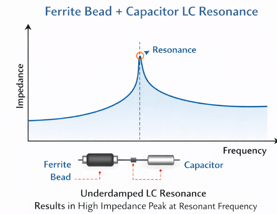
12. "More ferrites always means better noise performance."
Ferrite beads present increasing impedance with frequency and are used to attenuate high-frequency noise. They're useful when applied correctly. The problem is treating them as a universal fix.
A bead followed by a capacitor forms an LC filter whose Q factor can create a resonant peak that amplifies noise at the resonant frequency. Without damping, the "filter" makes things worse at certain frequencies. Additionally, ferrite beads on signal lines create frequency-dependent impedance changes that cause reflections on high-speed digital signals.
Where ferrites help: Isolating noisy power domains (with proper LC filter design including damping). Attenuating specific conducted EMI frequencies identified during testing. Placed near the noise source, not scattered randomly.
Where they don't help: Compensating for poor layout (large current loops, plane splits under fast signals, missing return paths). These are structural issues that ferrites cannot fix.
The Better Rule
Address noise at the source: minimize loop areas, maintain continuous return paths, control edge rates. Use ferrite beads as targeted filters for specific, identified noise problems. When you do use them, check the impedance curve against your actual noise frequencies and verify the LC interaction with downstream capacitance doesn't create a resonant peak.
Reference: Ott, H. "Electromagnetic Compatibility Engineering" on ferrite bead filter design and damping. Murata and TDK application notes on ferrite bead selection and LC resonance avoidance.
Vias, Impedance & Practical Design
13. "Any via stub is disastrous."
A via stub is the unused portion of a through-hole via when the signal transitions between inner layers. This stub acts as an unterminated transmission-line branch that reflects energy back into the signal path at its quarter-wave resonance frequency.
Example: 60-mil stub in FR-4 (εr ≈ 4.0)
f ≈ (3 × 10⁸) / (4 × 0.00152 × 2.0) ≈ 24.7 GHz
For a typical 62-mil (1.6 mm) board with a signal transitioning from layer 1 to layer 2, the stub length is roughly 55 mils. The quarter-wave resonance is approximately 27 GHz — well above the bandwidth of most digital signals, even multi-gigabit serial links. Note that degradation begins before the resonance frequency, so the practical impact threshold is lower, but for standard boards with signals up to a few GHz, through-hole vias are typically fine.
Stubs become a real problem on thick boards (>2 mm) with high-speed serial links. A 200-mil stub on a thick backplane has a resonance around 7.5 GHz — within the Nyquist frequency of 25 Gbps NRZ signaling.
When to ignore stubs: Signal bandwidth is well below the stub's quarter-wave resonance. Standard 1.6 mm boards with signals up to a few GHz.
When to address stubs: Thick boards with high-speed serial links (10 Gbps+). Backplane applications. Use back-drilling, controlled-depth drilling, or blind/buried vias.
The Better Rule
Calculate the stub resonance for your stackup and compare it to your signal bandwidth. If the resonance is more than 3× above your Nyquist frequency, the stub is not your problem. If it's within range, back-drill or use blind/buried vias. Don't avoid all vias — avoid stubs that resonate within your signal spectrum.
14. "If it works on a prototype, SI/PI must be fine."
A working prototype proves the design functions under the specific conditions of your lab: one board, one set of components, one temperature, one voltage. It does not prove the design has margin.
Manufacturing variation changes trace widths (affecting impedance), dielectric thickness (affecting delay and coupling), and copper roughness (affecting loss). Temperature shifts change switching speeds, dielectric constants, and conductor resistance. EMC testing is another common failure point — a board that functions on the bench can fail radiated emissions because return-path discontinuities and uncontrolled loops are efficient antennas.
The distinction is between "it works" and "it's designed with margin." A board with comfortable timing margin on its high-speed links tolerates variation. A board that's marginal in the lab is a production failure waiting for the right combination of conditions.
How to check margin without a full SI lab: Look at eye diagrams on the highest-speed links. Check for ringing and overshoot on fast buses. Measure power rail noise under load. If the vendor provides a channel compliance test (common for USB, PCIe, Ethernet), run it. These reveal whether you're operating with margin or on the edge.
The Better Rule
"It works" means you passed one test under one set of conditions. Check margin: run compliance tests if available, observe eye diagrams, measure rail noise. For low-volume products, this may be acceptable risk. For production volumes, it's a gamble on yield.
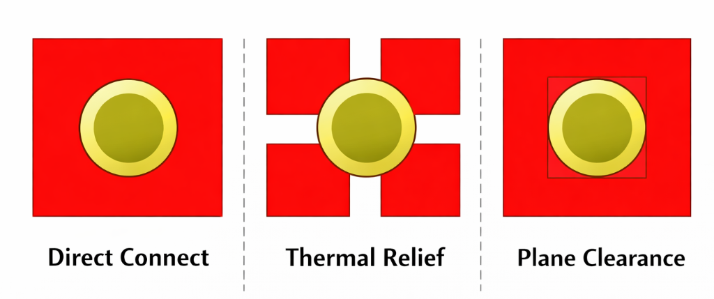
15. "Thermal relief on pads is always the right choice."
Thermal relief uses narrow spoke connections between a pad and a surrounding plane, restricting heat flow so the pad can reach soldering temperature during reflow or wave soldering.
When it causes problems: On high-current power pads, the narrow spokes limit copper cross-section for current flow, creating localized heating and increased resistance. On thermal/exposed pads (QFN, DFN packages), thermal relief defeats the thermal design by restricting the heat path from the IC die into the PCB — the IC manufacturer's thermal models assume a full copper connection. On decoupling capacitor ground pads, the added inductance from spoke connections increases loop inductance and reduces high-frequency effectiveness.
When to use: Standard signal-level through-hole and SMD pads connected to planes. Most pads on a typical board.
When to remove: High-current power pads (evaluate against IPC-2152). Thermal/exposed pads where thermal performance is critical. Ground vias for decoupling capacitors where minimizing loop inductance matters.
The Better Rule
Use thermal relief as the default for solderability. Explicitly remove it on pads where current capacity, thermal dissipation, or connection inductance is a design requirement. Your EDA tool lets you control this per pad — use that control.
Reference: IPC-2152 for current-carrying capacity calculations. IC vendor thermal application notes for exposed pad connection requirements (e.g., TI SLMA002, NXP AN11994).
The Common Thread
Every rule here started from a real engineering concern. The issue is context loss. A rule developed for a specific technology or speed range gets repeated without the conditions that made it valid. The better approach: understand the physics, evaluate whether the conditions apply to your design, and decide based on your actual constraints.
Rules of thumb are useful starting points. They become dangerous only when they replace engineering judgment.
| Rule | When It Holds | When It Doesn't |
|---|---|---|
| No 90° corners | Controlled-impedance, RF, HV | Most digital, power, non-impedance nets |
| Always serpentine to match | Tight-timing buses, protocol-required skew | When topology matching is sufficient |
| Everything is 50 Ω | RF systems, test interfaces | USB (90 Ω), PCIe (85 Ω), Ethernet (100 Ω), non-impedance nets |
| Clock frequency = speed | Never — rise time determines bandwidth | Always think in terms of edge rate |
| No termination at low freq | Short traces relative to rise time | Fast edges + long traces at any clock rate |
| Split analog/digital ground | True galvanic isolation requirements | Most mixed-signal — solid plane with partitioned layout |
| Pour everywhere | Stitched, well-referenced pour | Floating islands, narrow slots, unmanaged inner-layer pour |
| Guard traces reduce crosstalk | Properly stitched at close intervals | Floating or endpoint-only grounded traces |
| Diff pair doesn't need a plane | Never on PCB — coupling is limited | Always provide a continuous reference plane |
| Three-decade decap rule | Rough starting point if no other guidance | When it creates anti-resonance; follow IC vendor specs |
| Cap placement is everything | Loosely coupled plane pairs | Tightly coupled planes — via loop inductance dominates |
| More ferrites = less noise | Targeted filtering of identified frequencies | Compensating for layout problems; undamped LC resonance |
| All via stubs are bad | Thick boards + high-speed serial links | Standard 1.6 mm boards with sub-GHz bandwidth |
| Working prototype = good design | Never — one sample, one condition | Always verify margin for production confidence |
| Always use thermal relief | Standard signal pads for solderability | High-current, thermal pads, decap ground vias |
Frequently Asked Questions
Are these rules completely wrong?
No. Every rule here started from a real engineering problem. The issue is applying them as absolutes without evaluating whether the underlying conditions apply to your specific design.
How do I know which rules matter for my board?
Start with a quick triage. Identify the fastest interfaces by rise time, not clock frequency. Determine critical trace lengths. Review your stackup for reference plane continuity. For electrically short nets without impedance control requirements, most of these rules have minimal impact. For nets with fast edges over long traces on controlled-impedance stackups, all of them matter.
Should I worry about 90° corners on my GPIO traces?
Almost certainly not. For non-impedance-controlled traces with moderate edge rates and short lengths, the corner geometry has negligible electrical impact. Use 45° or arcs on your controlled-impedance nets and don't over-constrain the rest of your routing.
My prototype works — is that enough?
It depends on your production volume and risk tolerance. For a one-off prototype, a working board may be sufficient. For production, you need margin against manufacturing variation, temperature, and voltage extremes. Measure what you can — eye diagrams, rail noise, compliance tests — and make an informed decision.
Where can I learn more about the physics behind these rules?
Eric Bogatin's "Signal and Power Integrity — Simplified" covers most of the transmission-line, return-path, and PDN concepts here. Henry Ott's "Electromagnetic Compatibility Engineering" is the standard for EMC design practices. Howard Johnson and Martin Graham's "High-Speed Digital Design" provides quantitative analysis of many of these effects. IPC-2152 (current capacity) and IPC-2221 (design standard) provide manufacturing-grounded guidance. For specific interfaces, protocol specification documents from USB-IF, PCI-SIG, and JEDEC define the actual requirements your design must meet.
Want to Learn More About PCB Design Best Practices?
Check out our other blogs where we share practical PCB design insights, case studies, and real-world engineering approaches.
Read More PCB Design Insights Request Technical Discussion