Quick Navigation
- 1. Introduction
- 2. Why Thermal Simulation Matters
- 3. Thermal Fundamentals
- 4. Define the Goal
- 5. Where It Fits in the Design Flow
- 6. Choose the Model Scope
- 7. Collect the Required Inputs
- 8. Estimate Power Dissipation
- 9. Materials, Stackup, and Copper
- 10. Boundary Conditions
- 11. Model Fidelity
- 12. Critical Components and Hotspots
- 13. Step-by-Step Plan
- 14. Common Mistakes
- 15. Validation and Testing
- 16. Tools and Automation
- 17. Conclusion
- 18. FAQ
Key Thermal Planning Steps
- Define clear simulation objectives and pass-fail criteria before starting
- Collect realistic power dissipation data for all critical components
- Choose model scope based on thermal risk and component interaction
- Set boundary conditions that match the real operating environment
- Plan validation with prototype measurements before trusting absolute numbers
- Document assumptions so the model can be refined later without guesswork
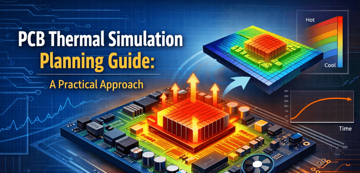
Introduction to PCB Thermal Simulation and Thermal Analysis
PCB thermal simulation predicts how heat moves through packages, copper, vias, dielectric material, air, and nearby mechanical structures. A useful thermal study does more than identify the hottest part. It explains why the hotspot forms, how heat spreads across the board, and whether the design is likely to stay inside safe operating limits before hardware is built.
What PCB Thermal Simulation Actually Tells You
A well-planned PCB thermal analysis helps answer practical design questions: whether a PMIC needs more copper, whether a processor sits in a weak airflow zone, whether thermal vias are doing meaningful work, or whether the enclosure will trap heat once the board leaves the bench. That is why planning matters as much as solver choice.
Why Planning the Simulation Matters Before You Start
Many thermal simulations fail because the setup is weak, not because the solver is weak. If the dissipation numbers are unrealistic, the copper model is oversimplified, or the airflow assumptions are wrong, the output can look precise while still being misleading. Planning first forces the team to define the question, collect the right inputs, and avoid spending time on a model that does not match the real product.
What This Guide Covers
This guide covers goals, scope selection, input collection, power estimation, material assumptions, boundary conditions, model fidelity, hotspot identification, validation strategy, and the common mistakes that cause simulation results to diverge from lab measurements.
Why PCB Thermal Simulation Matters in PCB Design
Preventing Hotspots and Reliability Problems
Excess heat is one of the fastest ways to reduce reliability in electronic systems. High local temperatures accelerate semiconductor aging, stress solder joints, dry out capacitors, reduce magnetic performance, and create large temperature gradients across the PCB. Thermal simulation helps expose these risks before they become repeated test failures, derating problems, or field returns.
Supporting Better Placement and Cooling Decisions
Thermal behavior depends heavily on placement, copper area, airflow path, heatsink contact, and enclosure constraints. Running analysis early helps decide whether a processor should move toward a board edge, whether a regulator needs more spreading copper, or whether a taller heatsink is worth the mechanical tradeoff.
Reducing Risk Before Prototype Testing
Simulation does not replace measurement, but it reduces risk before physical testing begins. It helps the team choose thermocouple locations, identify the components that deserve special attention, and define which operating conditions are most likely to expose thermal weakness during chamber or soak testing.
PCB Thermal Simulation Fundamentals
Heat Flow Through Components, Copper, and Air
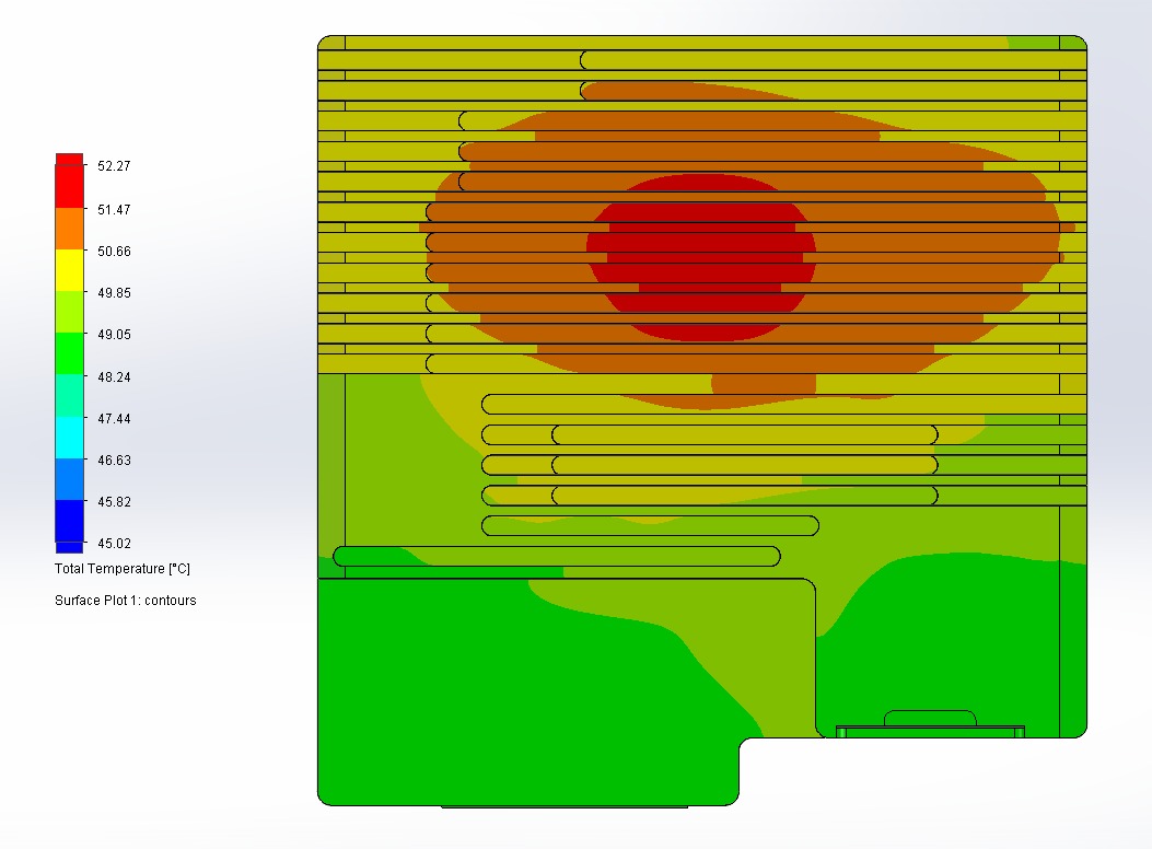
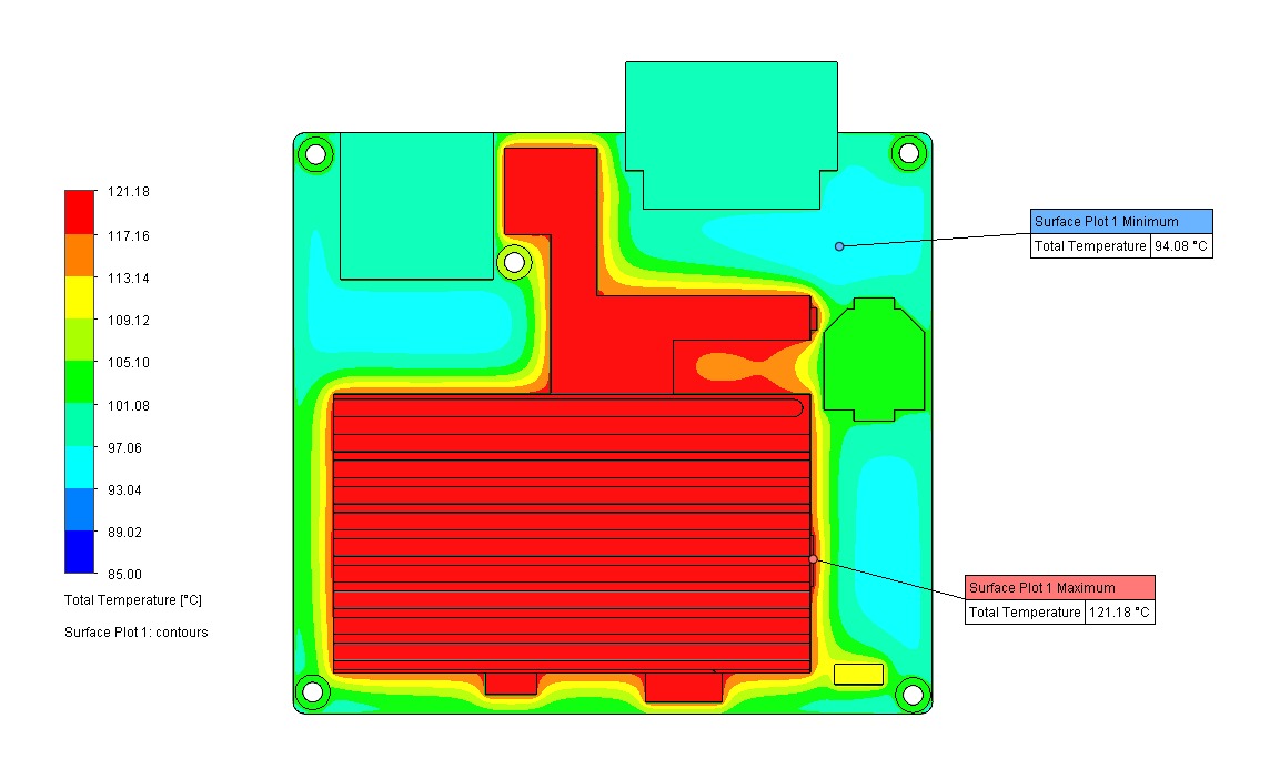
Heat generated inside a component leaves through multiple paths. Some travels through the package body, some through leads or pads into copper planes, and some into surrounding air. The board itself can become a significant heat spreader, but that depends on stackup, plane continuity, via density, and local congestion. The hottest part of the design is often limited by the nearby layout, not just by the package.
Junction Temperature, Case Temperature, and Ambient Temperature
One of the most common sources of confusion in thermal analysis is mixing up temperature definitions. Junction temperature is inside the die and usually sets the reliability limit. Case temperature is measured at a defined point on the package surface. Ambient temperature is the surrounding air or local reference temperature used by the model. A package-top measurement should never be treated as equal to junction temperature unless the thermal path is clearly understood.
Conduction, Convection, and Radiation in PCB Analysis
Most board-level models are dominated by conduction through solids and convection to air. Radiation is usually smaller at moderate temperatures, though it can matter in enclosed or higher-temperature systems. Because convection assumptions carry a lot of uncertainty, they should be chosen conservatively and validated whenever possible.
Define the Goal of the Thermal Simulation
Checking Maximum Junction Temperature
In many projects the primary goal is verifying that critical devices stay below maximum allowable junction temperature. This is common for processors, PMICs, memory, transceivers, motor drivers, and power semiconductors. If that is the goal, the model must focus on realistic dissipation, package properties, and the local cooling path around those devices.
Finding Board-Level Hotspots
Some studies are less about pass-fail limits and more about mapping where heat accumulates across the board. That is valuable when several moderate-power parts interact thermally, when connectors or plastics may run hot, or when large copper regions spread heat into unexpected areas.
Comparing Cooling Strategies and Layout Options
Thermal simulation is also useful as a comparison tool. Engineers can evaluate different heatsinks, copper pours, via arrays, airflow directions, or placement options without building multiple hardware variants. The most useful comparison studies keep assumptions consistent so the relative differences remain meaningful.
Evaluating Worst-Case Operating Conditions
A board that survives nominal room-temperature operation can still fail at high ambient, low airflow, maximum load, or inside an enclosure heated by neighboring hardware. Thermal planning should therefore include worst-case operating scenarios, not just a single nominal case.
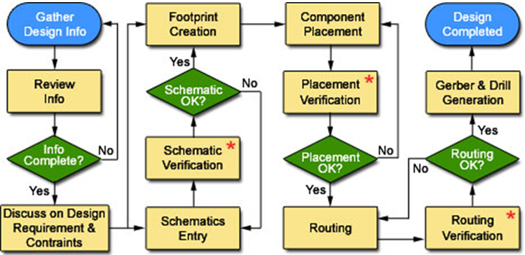
When Should You Plan Thermal Simulation in the PCB Design Flow?
Planning During Architecture and Component Selection
Thermal thinking should start before layout, not after a problem appears. During architecture and component selection, the team already knows which parts will dissipate meaningful power, which packages have weak thermal paths, and whether the product is enclosed, fan-cooled, or passively cooled.
Reviewing Thermal Risk During Placement
Placement is one of the highest-impact phases for thermal behavior. High-power components placed too close together can trap heat, while poor placement can block airflow or cut off access to spreading copper. A review during placement catches problems before routing makes them expensive.
Using Simulation Before Final Layout Freeze
A formal simulation pass before layout freeze helps confirm that the board is likely to meet thermal goals under expected operating conditions. At this stage the stackup, copper regions, and component positions are defined well enough to build a meaningful model, but changes are still practical.
Correlating Simulation After Prototype Testing
After prototypes are available, measured data should improve the model. That may mean updating airflow assumptions, correcting power numbers, or refining board-to-heatsink contact. Correlation does not mean forcing the model to match one point. It means making the model more realistic so later decisions based on it are trustworthy.
Choose the Scope of the Thermal Simulation Model
Component-Level vs Board-Level Simulation
The first scope decision is whether the problem is local or system-wide. A component-level model may be enough when the concern is a single device with a known dissipation path. A board-level model is better when multiple components interact, when copper spreading matters, or when the thermal path depends on overall layout.
Region-Based vs Full-Board Modeling
Not every study requires the entire board. A region-based model can save runtime and memory when the area of interest is limited to one processor, regulator cluster, or high-current section. But cutting the model too aggressively can remove the heat-spreading paths that actually control the result. If distant copper planes, mechanical supports, or airflow patterns affect the outcome, a full-board model may be necessary.
When to Include the Enclosure and Mechanical Parts
A bare-board model is often optimistic. Real products may sit inside plastic or metal enclosures, mount to chassis structures, or operate near insulation, batteries, cables, or other obstructions. If these elements influence airflow or create additional thermal paths, they should be included or at least approximated.
Balancing Accuracy, Runtime, and Model Complexity
More detail is not always better. The right model is detailed enough to answer the design question, but not so detailed that setup becomes slow and uncertain. Match model scope to design risk: simple models for screening, higher fidelity only when the outcome changes real design decisions.
Collect the Required Inputs Before Simulation
Board Stackup and Material Data
Thermal behavior depends heavily on stackup. Layer count, copper weight, dielectric thickness, prepreg arrangement, and board material properties all influence how heat spreads vertically and laterally. If exact material conductivity is unavailable, document the assumed values clearly so they can be revisited later.
Copper Planes, Pours, and Thermal Vias
Copper is often the dominant heat-spreading path on a PCB. Power planes, ground pours, stitched regions, and via farms can greatly reduce local thermal resistance, but only if they are actually connected in a useful way. The model should reflect whether copper is continuous, slotted, necked down, or interrupted by routing and keep-out areas.
Component Package Information and Thermal Resistance Data
Packages differ widely in how they reject heat. Exposed-pad QFNs, BGAs, power packages, and molded modules each have different dominant heat paths. Datasheet values such as junction-to-ambient or junction-to-board resistance can provide guidance, but they are not a substitute for a board-specific model.
Exposed Pad Soldering and Voiding Effects
For QFN, DFN, and other thermal-pad packages, solder void percentage under the exposed pad directly affects thermal resistance to the board. Industry guidance often treats up to 50% voiding as acceptable for general applications, but high-power devices can see junction temperature rise by 10-15°C when pad wetting is poor. Conservative simulations should account for realistic contact quality rather than assuming perfect wetting, especially for processors, PMICs, and RF power devices.
Power Dissipation and Operating Modes
One of the most important inputs is device power dissipation under real use conditions. This can vary by mode, duty cycle, load, supply voltage, clocking, and ambient environment. A single worst-case number may be enough for a quick screen, but detailed studies should cover multiple scenarios.
Ambient, Airflow, and Mounting Conditions
Ambient temperature alone is not enough. The model should define whether the product is naturally cooled or fan-cooled, vertical or horizontal, enclosed or open, and whether it mounts to brackets, thermal pads, aluminum structures, or a larger assembly that alters heat flow.
Estimate Component Power Dissipation Correctly
Using Datasheet Values Carefully
Datasheets may list typical current, maximum current, thermal resistance values, and example power numbers, but those figures are usually measured under conditions that differ from the final application. Treat them as guidance, not as numbers to copy blindly into the model.
Estimating Real Power from Load Conditions
The most credible power estimates come from actual operating conditions. For regulators, drivers, and processors, that means calculating or measuring power from supply voltage, efficiency, switching losses, load profile, and duty cycle. If exact numbers are unknown, simulate a defensible range instead of one convenient value.
Accounting for Startup, Peak, and Continuous Power
Not all thermal risk comes from steady-state operation. Some boards experience short bursts of high power during boot, communications peaks, motor startup, or battery charging. If those events are frequent or long enough to heat the system meaningfully, they belong in the plan.
Common Errors in Power Assumptions
Typical mistakes include using input power instead of dissipated power, ignoring conversion efficiency, assuming all devices operate at full load continuously, or forgetting that nearby components raise the local thermal environment even when they are not individually critical. These errors can dominate the final thermal result more than solver choice.
Define Material Properties, Stackup, and Copper Details
FR-4 and Material Thermal Conductivity Assumptions
Most PCB simulations begin with FR-4, but real laminate systems vary. Thermal conductivity depends on resin system, filler content, fiber orientation, and whether the board uses standard or specialized materials. Even when exact values are unavailable, recording the assumed conductivity range improves traceability.
Copper Thickness and Plane Spreading Effects
Copper weight strongly affects heat spreading. Thicker copper usually lowers local thermal resistance and distributes heat across a wider area, but only when the copper is continuous enough to act as a true spreader. Narrow bottlenecks, isolated islands, and split planes reduce that benefit. Copper traces also generate heat when carrying current, and that self-heating adds to the local thermal load. IPC-2152 is the better reference for current-carrying capacity on power paths because it reflects trace width, thickness, temperature rise, and nearby copper more realistically than the older IPC-2221 charts.
The Impact of Vias, Pads, and Large Copper Regions
Vias can dramatically improve vertical heat transfer between layers, especially under exposed-pad packages and power devices. Pads and nearby planes also matter because they form the first escape path from the package into the board. If the goal is hotspot accuracy around a critical component, those details should not be simplified too aggressively.
Power Plane Splits and Thermal Barriers
A split in a ground or power plane can behave like an unintended thermal barrier, concentrating heat on one side and blocking lateral spreading. Plane splits may still be necessary for signal isolation, noise reduction, or voltage-domain separation, but their thermal consequences should be reviewed before simulation. If a high-power component sits near a split, the model should capture that discontinuity rather than assume continuous copper. In some layouts, thermal vias or copper stitching across the split may be needed to restore the spreading path.
When Simplified Material Models Are Acceptable
Simplified material models are acceptable during early screening when the goal is comparison rather than absolute prediction. They become risky when the design is close to thermal limits or when the board relies heavily on local geometry to remove heat.
Set Boundary Conditions and Ambient Assumptions
Choosing the Right Ambient Temperature
Ambient temperature should represent the real environment seen by the product, not the most convenient room-temperature value. In many systems the air around the PCB is already elevated by enclosure heating, nearby power devices, or poor ventilation.
Natural Convection vs Forced Airflow
Airflow assumptions can change results dramatically. A naturally cooled board behaves very differently from one placed in a forced-air stream. If fan operation, vent placement, or orientation is uncertain, simulate more than one airflow case rather than relying on a single nominal assumption.
Board Orientation and Natural Convection Effects
Board orientation matters. A vertically mounted board usually cools better than a horizontal one because vertical orientation promotes stronger buoyancy-driven airflow. Horizontal boards with components facing downward can perform worse still because heat is more easily trapped under the assembly. In naturally cooled products, the difference between orientations can be 15-20°C on the same component. If the final product orientation is not fixed yet, the safer choice is simulating the worst realistic orientation.
Modeling Heatsinks, Chassis Contact, and Mounting
Heatsinks and mechanical contact surfaces are often modeled too optimistically. Real contact resistance, thermal interface material thickness, fastener pressure, pad compression, flatness, and assembly tolerance can all change the effective cooling path. Conservative approximations are usually better than idealized ones unless measured data is available.
Thermal Interface Material Selection and Modeling
TIM conductivity matters, but bond-line thickness matters just as much. Basic pads may be near 1 W/m.K while premium gap fillers or phase-change materials can exceed 5 W/m.K, yet a thin layer of moderate-conductivity material can still outperform a thick layer of higher-conductivity material. If TIM choice is still uncertain, simulate multiple scenarios so the design team understands sensitivity before mechanical decisions are locked.
Avoiding Unrealistic Boundary Conditions
Ideal heatsink contact, aggressive convection coefficients, and perfectly uniform ambient exposure can make a thermal model look much better than the real product. Boundary conditions should reflect how the board is actually mounted, cooled, and used.
Decide the Right Level of Model Fidelity
When a Simplified Model Is Good Enough
Simplified models are useful early in development when the goal is ranking options, identifying likely hotspots, or estimating whether a design is clearly safe or clearly risky. They are faster to build and easier to adjust as the design evolves.
When Detailed Local Geometry Should Be Included
Detailed local geometry becomes important when pads, copper pours, exposed thermal pads, via farms, or nearby cutouts strongly influence temperature rise. If a few degrees determine whether the design passes, local detail deserves more attention.
How Much of the Copper and Pad Region to Model
Around high-power devices, the immediate pad and copper region may dominate the thermal path. Including this detail can improve confidence, especially for processors and power packages mounted over dense spreading planes. The question is always whether more detail changes the decision being made, rather than simply making the model harder to manage.
Managing Simulation Memory and Runtime
Large models become expensive quickly. Manage runtime by focusing detail where it matters most, simplifying distant features with limited thermal influence, and using staged analysis where a coarse model identifies the zones that justify refinement.
Identify Critical Components and Hotspot Areas
Processors, PMICs, Transceivers, and Power Devices
These components usually deserve the first thermal review because they combine meaningful dissipation with strict operating limits. Their temperatures are also influenced by board-level interactions, not just by package rating.
Dense Copper Bottlenecks and Heat Accumulation Areas
Heat does not always build up only at the power component itself. It can accumulate where multiple devices feed the same copper region, where airflow is blocked, or where copper narrows before reaching a larger spreading area.
Connector, Enclosure, and Airflow Shadow Effects
Connectors, shields, plastics, and tall components can alter local airflow and create shadowed regions with weaker cooling. These interactions matter in compact products where board spacing is tight and convection paths are limited.
Prioritizing the Highest-Risk Thermal Regions
Not every warm component is equally important. Prioritize regions where high power, poor cooling, tight reliability limits, and measurement uncertainty all overlap. Those are the areas where thermal analysis delivers the most value.
Thermal Coupling Between Components
Components do not heat in isolation. A power MOSFET running warm can push nearby capacitors, crystals, or analog sections closer to their limits even if the MOSFET itself appears acceptable. This coupling matters even more when a higher-power device sits close to temperature-sensitive parts such as electrolytic capacitors, frequency-sensitive timing components, or precision analog circuitry. As a practical screening rule, any component within roughly 10-15 mm of a significant heat source deserves closer thermal review. The model should capture these interaction zones rather than treating every device as an isolated source.
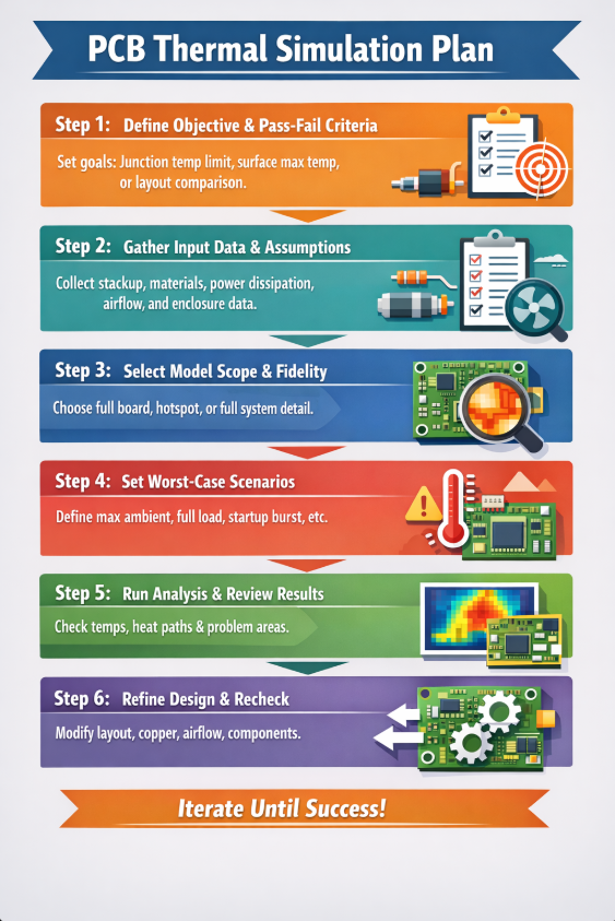
Build a Step-by-Step PCB Thermal Simulation Plan
Step 1: Define the Objective and Pass-Fail Criteria
Start by defining what the simulation must prove. This may be a junction-temperature limit, a maximum surface temperature, a heatsink target, or a comparison between two layouts. Clear pass-fail criteria keep the study focused.
Step 2: Gather Input Data and Assumptions
Collect stackup information, material properties, package data, estimated power dissipation, airflow conditions, and enclosure assumptions. Document which values are exact and which are approximate.
Step 3: Select Model Scope and Fidelity
Decide whether the model should cover one hotspot region, the full board, or the board plus enclosure. Then choose how much local detail is needed around critical components.
Step 4: Set Scenarios for Worst-Case Operation
Define the operating cases to simulate, such as maximum ambient, reduced airflow, continuous full load, startup burst, or enclosure-heated conditions. The study is only as useful as the scenarios it includes.
Step 5: Run the Analysis and Review Results
Review not only the hottest temperatures but also the path causing them. Identify whether the issue is driven by dissipation, placement, copper limitation, heatsink contact, or weak boundary assumptions.
Step 6: Refine the Design and Recheck
Use the results to change the design. That may mean moving components, increasing copper area, adding vias, improving chassis contact, changing airflow strategy, or selecting a different package. Re-run the model after meaningful changes rather than treating the first pass as the final answer.
Common Mistakes When Planning Thermal Simulation on a PCB
Common Mistakes
- Using incorrect power numbers
- Ignoring real airflow and enclosure effects
- Confusing surface temperature with junction temperature
- Over-simplifying or overcomplicating the model
- Skipping correlation with measured data
Best Practices
- Calculate power from actual operating conditions
- Model realistic airflow and enclosure constraints
- Understand measurement locations before comparing numbers
- Match model detail to the design question
- Validate simulation against prototype data
Using Incorrect Power Numbers
Wrong dissipation estimates can invalidate the entire simulation. This is one of the most common reasons predicted and measured temperatures do not agree.
Ignoring Real Airflow and Enclosure Effects
A board tested in open air may behave very differently once it sits inside the final enclosure. Ignoring this usually leads to optimistic results and late-stage surprises.
Confusing Surface Temperature with Junction Temperature
Measured surface temperature, heatsink temperature, and internal junction temperature are not interchangeable. Misreading them can create either false confidence or unnecessary redesign.
Over-Simplifying or Overcomplicating the Model
A model that is too simple may miss the dominant thermal path, while a model that is too detailed may consume time without improving design decisions. The best model is the one matched to the engineering question.
Skipping Correlation with Measured Data
Even a well-built simulation should be checked against real measurements whenever possible. Correlation is what turns a one-time thermal study into a reliable design tool.
How to Validate Thermal Simulation Results with Real Testing
Thermocouples, IR Cameras, and Chamber Testing
Validation usually combines direct contact measurements, infrared inspection, and controlled environmental testing. Each method has strengths and limitations, so results should be interpreted in context rather than taken at face value.
How to Compare Measured and Simulated Temperatures
Compare like with like. If the simulation reports junction temperature but the lab measures package-top or heatsink temperature, conversion and thermal-path interpretation are required before concluding that the model is wrong.
Explaining Differences Between Lab and Simulation Results
Differences often come from inaccurate power estimates, simplified contact resistance, airflow mismatch, sensor placement, IR emissivity errors, or normal manufacturing variation. The goal is to understand the cause, not to force the two data sets to match superficially.
Improving Correlation Over Multiple Iterations
Thermal models become more useful as they are updated with better data. A disciplined loop between simulation and testing turns thermal analysis from a checkbox exercise into a design asset.
Thermal Simulation Tools and Automation Approaches
Board-Level Thermal Tools and Solver Options
Different tools target different needs. Some are optimized for board-level screening, others for detailed CFD or enclosure interaction. The right choice depends on whether the problem is local, board-wide, or tightly coupled to airflow behavior.
When to Use Simplified PCB Thermal Analysis
Simplified analysis is useful when the goal is quick comparison, early feasibility checking, or deciding which parts of the design need a deeper review. It is often the best first step.
When CFD or Enclosure-Level Analysis Is Needed
If airflow path, fan placement, vent geometry, chassis conduction, or multi-board interaction dominate thermal behavior, enclosure-level simulation may be necessary. This is common in compact electronics, automotive systems, industrial control boxes, and fan-assisted products.
How Automation Can Improve Thermal Planning
Automation can help organize inputs, track assumptions, flag high-risk components, compare revisions, and reduce manual setup effort. AI-assisted workflows are useful for screening likely hotspots, ranking likely risk by power dissipation, package type, and local copper availability, and summarizing thermal risk before a full model is built. Final design decisions still need engineering review and measured validation.
Conclusion and Thermal Planning Checklist
Key Questions to Answer Before Running a Simulation
Before launching a solver, the team should know what must be proven, which components are critical, what power levels are realistic, what boundary conditions apply, and how results will be validated later. If those questions are unclear, the simulation is probably being started too early.
A Simple Thermal Planning Checklist for PCB Teams
- Define the objective and pass-fail criteria
- Identify critical components and thermal risk areas
- Collect stackup and material data
- Estimate power dissipation by operating mode
- Choose appropriate model scope and fidelity
- Set realistic airflow and ambient conditions
- Run worst-case operating scenarios
- Review hotspots and thermal paths
- Compare the model against measurements when hardware is available
Best Practices for More Reliable Thermal Results
The most reliable PCB thermal simulations are planned early, built from realistic assumptions, kept aligned with the actual product environment, and improved through measurement correlation. Good thermal analysis is valuable when it guides design tradeoffs, not when it simply produces a colorful report.
Frequently Asked Questions
Want to Learn More About PCB Design Best Practices?
Explore more of our blogs on thermal planning, signal integrity, power integrity, verification, and design automation across Altium, KiCad, and other PCB workflows.
Explore Our Blog Request Technical Discussion