The Electronic Battlefield: What We're Really Up Against
Let's talk about the numbers nobody wants to discuss. These aren't marketing statistics—they're the harsh realities I've learned from years of PCB autopsies and late-night debugging sessions.
Silicon Labs AN895
Analog Devices ADP1763
(Many 3.3V families: 1.71-3.6V)
Electronics Cooling
🚨 The Reality of Modern Electronics
Electronics have become incredibly complex. A modern PCB isn't just a circuit—it's a system where multiple subsystems must work together reliably. Power domains, signal integrity, thermal management, EMI control... there are many potential failure modes to consider.
Understanding these failure mechanisms helps you design more robust systems that can handle real-world operating conditions.
Killer #1: The ESD Assassin ⚡
Electrostatic Discharge (ESD)
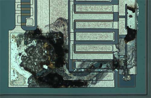
How it kills: High voltage ESD events can permanently damage semiconductor junctions, creating latent failures that manifest weeks or months later. Test standards like IEC 61000-4-2 specify up to 15kV air discharge for system-level immunity testing.
The stealth factor: Repeated ESD events and latent damage are well-documented; effects are device- and stress-dependent. Your circuit works perfectly after assembly, passes all tests, then mysteriously fails in the field due to accumulated ESD stress.
| ESD Voltage Source | Typical Range (depends on humidity) | What's at Risk |
|---|---|---|
| Walking on carpet | 1.5-35kV (low to high humidity) | CMOS inputs, microcontroller pins |
| Removing tape from roll | 2-20kV | Analog front-ends, ADCs |
| Handling plastic materials | 1-15kV | Op-amps, precision references |
| Human body (dry conditions) | 2-8kV | Any unprotected IC pin |
Ranges strongly depend on RH/materials; adapted from ESDA examples.
🛡️ Survival Strategy
ESD protection diodes on all external connections, proper grounding, and ESD-safe handling procedures. But here's what nobody tells you: even protected circuits can suffer cumulative ESD damage that degrades performance over time.

Killer #2: The Temperature Executioner 🔥
Thermal Stress
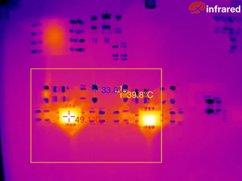
How it kills: Heat accelerates failure mechanisms in electronics. Many commercial parts specify Tj(max) 125–150°C; design to keep Tj comfortably below the datasheet maximum. The widely-used "10°C rule" suggests component life roughly halves for every 10°C increase, though this rule-of-thumb varies significantly by failure mechanism and is most applicable to certain chemistries like electrolytic capacitors.
The cascade effect: One overheating component increases ambient temperature, stressing nearby components, which then generate more heat, accelerating degradation.
- Electrolytic capacitor aging: ESR increases with temperature, ripple voltage rises
- Solder joint fatigue: Thermal cycling creates micro-cracks, intermittent connections
- IC parameter drift: Precision circuits lose accuracy, timing circuits drift
- PCB substrate stress: High temperatures can cause delamination and trace lifting
⚠️ The Silent Temperature Killers
- Poor via stitching: Heat trapped in copper layers with no escape path
- Inadequate copper pour: Current bottlenecks create hot spots you never calculated
- Component clustering: Multiple heat sources in small area overwhelming thermal capacity
- Missing thermal vias: Power components with no heat path to ground plane

Killer #3: The Power Supply Strangler ⚡
Power Distribution Network Issues
How it kills: Each IC has specific operating voltage ranges and noise tolerance requirements. Many modern microcontrollers operate from 1.71V to 3.6V, while others have tighter specifications. Power supply noise, voltage drops, and current spikes create stress that accumulates over time.
The invisible killers:
- Ground bounce: High-speed switching creates voltage spikes and transients that can trigger latch-up in CMOS devices (see JESD78)
- Power supply droop: Insufficient decoupling causes voltage dips during current spikes
- Current density violations: Traces carrying more current than their width can handle
- Via impedance: Use multiple short vias at each decoupler; avoid sharing vias among caps
🛡️ Power Distribution Best Practices
Adequate decoupling (bulk + ceramic), proper power plane design with via stitching, and current density calculations for all power traces. Use multiple short vias near decoupling capacitor pads to minimize loop inductance. Size and count vias according to current requirements and follow IPC-2152 guidance for current-carrying capacity.
Reference: TI Power Distribution Network Design
Killer #4: The EMI/EMC Phantom 📡
Electromagnetic Interference
How it kills: EMI typically causes functional upsets—logic errors, data corruption, and analog circuit instability. While EMI itself doesn't usually cause permanent damage, the transients and noise that accompany EMI can trigger latch-up conditions or electrical overstress that may permanently damage components. Fast transients (ESD/EFT/overshoot) can trigger latch-up (see TI Latch-up Guide).
The interference sources:
- Clock signal radiation: High-speed edges couple into sensitive circuits
- Ground loops: Multiple ground connections create antenna structures
- Uncontrolled impedances: Reflections and ringing stress digital inputs
- Power supply switching noise: Coupling through shared power/ground
Killer #5: The Manufacturing Saboteur 🏭
Process-Induced Failures
How it kills: Manufacturing defects create latent failures—weak solder joints, contamination, and process damage that manifest as field failures months after production.
| Manufacturing Issue | Immediate Symptom | Long-term Killer |
|---|---|---|
| Cold solder joints | Often none (works initially) | Intermittent connections, total failure |
| Flux residue | Often none visible | Corrosion, leakage currents |
| Via barrel cracks | Passes connectivity test | Thermal cycling causes open circuit |
| Component stress | Works within spec | Accelerated aging, parameter drift |

Killer #6: The Environmental Assassins 🌍
Moisture, Corrosion, and Contamination
How they kill: Environmental factors create electrochemical reactions that slowly dissolve your circuit traces, degrade insulation, and create conductive paths where none should exist.
- Humidity absorption: PCB substrates absorb moisture, reducing insulation resistance
- Salt contamination: Creates conductive paths, accelerates corrosion
- UV degradation: Breaks down plastic components, changes electrical properties
- Chemical exposure: Cleaning solvents, flux, even skin oils cause long-term damage
🌊 Environmental Degradation Process
The progression of moisture-related damage varies significantly with humidity levels, contamination, applied bias voltage, trace spacing, and temperature. Standard test conditions like Temperature-Humidity-Bias (THB) typically run hundreds to thousands of hours to evaluate electrochemical migration and conductive anodic filament formation. The actual time to failure depends heavily on these environmental and design factors.
Killer #7: The Human Factor 👥
Assembly and Testing Damage
How it kills: Physical damage during handling, probe contact damage during testing, and mechanical stress from connectors and cables create failure sites that worsen over time.
- Test probe damage: Sharp probes scratch protective coatings, create corrosion sites
- Connector stress: Repeated insertion/removal cycles cause trace lifting
- Component handling: Static-sensitive devices damaged during manual placement
- Rework damage: Heat damage to adjacent components during repairs
Survival Strategies: Fighting Back Against the Killers 🛡️
Understanding what kills electronics is the first step to keeping them alive. Here are the defensive strategies that actually work:
Design for Survival
- Derating: Never run components at their maximum ratings—use 70% rule
- Redundancy: Multiple power paths, backup circuits for critical functions
- Protection: TVS diodes, fuses, current limiting on all external interfaces
- Thermal management: Via stitching, thermal vias, adequate copper coverage
- Ground integrity: Solid ground plane, strategic ground connections
Manufacturing Defense
- DFM rules: Design rules that prevent manufacturing-induced failures
- Test accessibility: Proper test points that don't damage the circuit
- Assembly constraints: Component spacing that prevents stress damage
- Quality control: Inspection points that catch latent defects
🎯 The Ultimate Survival Rule
Assume everything will try to kill your electronics—design defensively, test aggressively, and never trust that "it worked yesterday" means it will work tomorrow.
Battle Scars: When the Silent Killers Struck 💥
Theory is one thing. Reality is brutal. Here are real war stories from the PCB trenches—personal encounters with the electronic killers that turned working prototypes into expensive lessons.
The Power-Ground Assassin
The Setup: A perfectly working prototype, tested and ready for production. Everything checked out—until it didn't.
The Kill: Three different ways this silent killer struck:
- Library Symbol Sabotage: An incorrect symbol in the component library had power and ground pins swapped. The schematic looked perfect, the design passed all checks, but first power-up was the last power-up.
- Manufacturing Ambush: A fabrication error created an internal short between power and ground planes. The boards looked perfect from the outside, but every single one was DOA.
- Mechanical Execution: A mounting screw abraded through the soldermask, exposing a power trace. The screw was grounded to the enclosure. One installation later: instant short, magic smoke, project delayed by 6 weeks.
The Aftermath: Complete board respin, new fab run, and a very expensive lesson about the importance of power integrity verification at every level.
The Board-to-Board Connector Phantom
The Setup: Multi-board system with critical connections between PCBs. Each board worked perfectly in isolation.
The Kill: Mechanical tolerance stackup meant connectors didn't align properly. Some pins made intermittent contact, others were stressed beyond their limits. The system would work, then fail randomly, creating the worst kind of debugging nightmare.
The Silent Part: The connection looked fine—it was electrically continuous during testing. But mechanical stress on the connector pins created microscopic cracks that became full opens under thermal cycling.
The Aftermath: Three board respins to get the mechanical positioning right, plus a complete connector strategy overhaul. Lesson learned: mechanical engineers and PCB designers need to work together from day one.
The FPGA Voltage Assassin
The Setup: High-performance FPGA design with multiple voltage domains. Careful power sequencing, proper decoupling, everything by the book.
The Kill: A stressed I/O pin on the FPGA was supposed to see 1.8V logic levels. Due to a level shifter design error, it received 3.3V instead. The FPGA's input protection clamped the voltage—but couldn't handle the current.
The Chain Reaction: The FPGA I/O pin shorted internally, creating a direct path from 3.3V to ground. This overloaded the power supply, which tripped its protection circuit. The entire system went dark, and the $200 FPGA became a silicon paperweight.
The Aftermath: Board respin with proper level shifting, additional current limiting, and paranoid voltage domain verification. One small voltage error killed the most expensive component on the board.
The Power Supply Strangler
The Setup: Custom switching power supply design, calculated for efficiency and cost optimization. Breadboard prototype worked perfectly.
The Kill: Two silent killers worked in concert:
- Design Oversight: The feedback compensation network was miscalculated, causing the power supply to oscillate instead of starting properly.
- Programming Error: A programmable power management IC had incorrect startup sequence parameters, preventing the enable signals from reaching the switching controller.
The Silent Part: The power supply would attempt to start, fail, retry, fail again—all silently. No error indicators, no debug outputs, just a dead system that looked like it should work.
The Aftermath: Complete power supply redesign and a new rule: always include diagnostic LEDs and test points for every critical power management function.
The Memory Corruption Phantom
The Setup: High-speed DDR memory interface, carefully routed with controlled impedance and proper termination. Timing simulation showed everything was within spec.
The Kill: Signal integrity issues caused random bit errors in memory transactions. The symptoms were subtle—occasional data corruption, rare system crashes, intermittent failures that seemed unrelated to memory.
The Silent Attack: The signal integrity problems were marginal—not bad enough to prevent the system from working, but bad enough to cause rare errors. These errors accumulated over time, corrupting data and making the system unreliable.
The Investigation: Weeks of debugging led to the discovery that via stubs on the memory traces were causing reflections. The reflections didn't prevent data transmission but occasionally corrupted it. Via-stub reflections → back-drilling/back-drill rule-checks (see Signal Integrity Journal).
The Aftermath: Board respin with back-drilling to remove via stubs, improved trace routing, and comprehensive signal integrity verification. A seemingly minor SI issue nearly killed the entire project.
🎯 The Common Thread
Every one of these failures had the same characteristics:
- Silent: No obvious symptoms until complete failure
- Subtle: Small design details with catastrophic consequences
- Expensive: Each respin cost weeks of time and thousands of dollars
- Preventable: Could have been caught with more comprehensive design verification
The Automation Advantage: Built-in Survival
These battle scars taught us something important: many of these failures could have been prevented with better design verification and embedded safety margins. While manual PCB design focuses on getting circuits to work, automated design systems can embed survival strategies from the beginning.
Modern PCB automation incorporates failure prevention directly into the design process, addressing many of the silent killers before they have a chance to strike:
- Partial automatic power integrity: Some verification to help reduce power/ground shorts and voltage domain errors
- Mechanical constraint checking: Helps prevent some board-to-board connectivity issues through basic spacing verification
- Basic voltage domain awareness: Simple level shifter considerations and basic voltage tolerance checking
- Standard power supply practices: Basic design rules for common startup sequences and compensation networks
- Improved signal integrity: Better controlled impedance routing and via management to help reduce memory corruption
- Manufacturing DFM rules: Standard design rules to help prevent some fabrication-induced failures
💡 The Lesson from the Trenches
Every respin taught us that it's cheaper to prevent failures than to debug them. The silent killers are predictable—they follow the same patterns, attack the same vulnerabilities, and create the same types of problems.
The solution isn't just better design practices—it's embedding those practices into your workflow from the start.
What I've Learned from Hardware Development
After many years of PCB design and debugging failed boards, here's what experience has taught me: electronic systems will eventually fail. Understanding the common failure mechanisms helps you design more reliable products.
The key insight isn't that failure is inevitable—it's that many failures follow predictable patterns.
The failure modes we've discussed—ESD damage, thermal stress, power distribution issues, EMI problems, manufacturing defects, and environmental factors—are well-documented in reliability literature. Each has characteristic signatures and preventable causes.
But here's what I wish I had understood earlier: experienced hardware engineers design defensively. They don't just ask "does it work?" but also "what could cause this to fail, and how do I prevent it?"
It's a methodical approach. Review datasheets carefully. Understand operating limits. Design with adequate margins. Test thoroughly under realistic conditions.
💬 Share Your Horror Stories
These are just some of the ways electronics can fail unexpectedly. Every hardware engineer has their own collection of mysterious failures and "it was working yesterday" moments.
What about you? What's the strangest way you've seen a PCB die?
Was it a component that failed for no apparent reason? A design that worked perfectly in testing but failed in production? A board that ran for months then suddenly stopped working?
Share your experiences in the comments below—other engineers can learn from your failures too.
Based on real hardware development experience and industry failure analysis data. Your mileage may vary, but the killers are definitely out there.
