
Quick Navigation
The Short Answer: Earlier Than You Think
Most engineers "discover" signal integrity when:
- The board is already routed, or
- The fab is asking for final Gerbers, or
- The prototype only works at reduced link speed
The Honest Answer
Start planning for signal integrity one phase earlier than you currently do.
If SI first shows up as a topic during routing, you are already late by at least two phases. You've already chosen interfaces and PHYs, fixed the stackup, and placed components—committing to channel lengths and via counts.
This blog examines the PCB project as a timeline and answers, phase by phase:
- What SI decisions must be made in this phase
- What happens if you push them later
- What you can safely ignore until later without taking silly risk
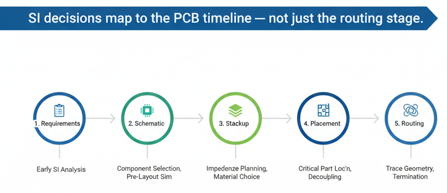
Phase 0: Requirements (Before Schematic)
This is the part most teams skip completely. They jump straight into schematic symbols and footprints. For SI, Phase 0 is where you quietly decide whether this is a "don't worry about it" board or a board where SI can easily cost a re-spin if you guess wrong.
Quick Data-Rate Question: Do You Even Need Serious SI?
You do not need a full SI workflow for every board. You do need a five-minute triage:
Ask yourself:
- What are the fastest interfaces on this board?
- GPIO, I²C, UART, low-speed SPI, slow parallel buses → usually low SI risk
- DDR2/DDR3/DDR4, LVDS display links, MIPI, USB 2.0 → moderate SI risk
- USB 3.x, PCIe, HDMI/DP, 1G/10G/25G Ethernet, custom SerDes → high SI risk
- Rough length of the high-speed paths?
- All critical links stay inside 2–3 cm on the same board, one connector at most → easier
- Long runs across the board, multiple connectors/backplane/cable → harder
- Are you doing something your team has never done before?
- New data rate (first time with PCIe Gen4 or 10G/25G)
- New form factor (thin board, very small, very dense)
- New stackup or material
- Are you planning to test the fastest interface?
- Plan and talk to the vendors how will you test the interface
- Test points, DDR4 interposers are areas which need sufficient investigation time
Risk Bucketing
From these answers you can bucket the project:
- No interfaces above ~100–200 MHz signal content
- Short traces, no exotic connectors
- Re-using a known-good architecture
- One or two moderate-speed interfaces (DDR3, LVDS, USB 2.0) but within a familiar range
- Board size and connectors are similar to previous, known-working designs
- Any multi-gigabit serial links, dense DDR4/DDR5, or multi-connector paths
- New speed grade or topology for your team
When You Must Budget for SI from Day 1
If the project lands in the high SI risk bucket, you cannot treat SI as "we'll see at layout."
You should explicitly budget, before opening the schematic:
- Stackup and material work: Talk to your fabricator about layer count, whether standard FR-4 is enough or mid-/low-loss material (FR408/Megtron6) is needed, and impedance control capability
- Advanced via strategy: Do you need backdrilled vias for long SerDes links or blind/buried microvias for dense BGAs?
- Rough channel budgets: Note max total route length and max number of connectors/vias the vendor allows
⚠️ What Happens If You Skip This
If you discover at routing time that the "default" 4-layer FR-4 stackup is giving trouble then it can have cascaded effect on the simulation. It is possible that new material brings in different trace widths, plane separations complying with which can cause delays.
Phase 1: Schematic Capture
In most teams, schematic capture is treated as a purely logical exercise: connect nets, pass ERC, done. From an SI point of view, schematic is where you quietly lock in how hard your life will be later.
Interface Selection That Locks in SI Difficulty
By the time schematic is "almost done," you have usually made these decisions:
- Which standards you will use (PCIe Gen3 vs Gen4 vs 10GBASE-KR)
- How wide each interface is (x1, x4, x8 links; 1-lane vs 4-lane LVDS)
- Which signals leave the board and via what kind of connector
Each Decision Has Concrete SI Effects
- A PCIe Gen4 x4 link between two BGAs on the same board is one thing
- The same link routed through a mezzanine connector to a daughtercard is a different, much stricter SI problem
- A 1-lane LVDS display link over a short cable is not the same risk level as a 4-lane MIPI link through a flex plus board
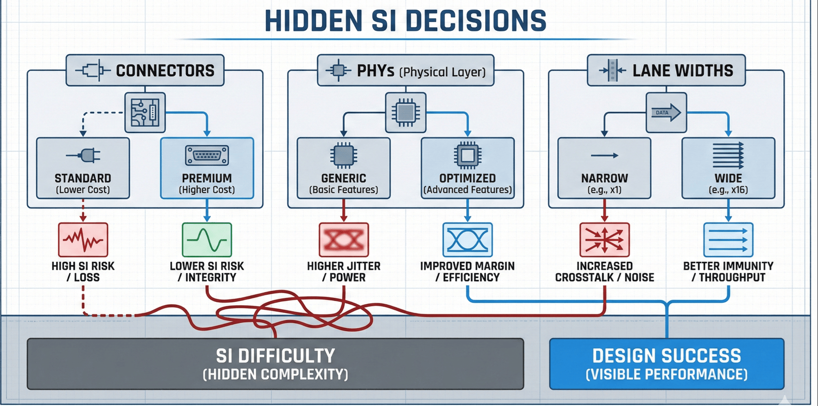
Component Choices That Silently Set SI Constraints
Several schematic decisions look harmless but lock in hard SI requirements:
1. PHY / Transceiver Choice
- Different PHYs for the same protocol can have different tolerance to loss, jitter, and skew
- Some have built-in equalization and good diagnostics; others are simpler
- Choosing "the cheapest PHY" without reading its layout/channel recommendations can box you into an impossible constraint set later
2. Package Types and Pinouts
- A SerDes in a tight BGA with poorly ordered pins may force extra vias and layer swaps
- A more SI-friendly pinout (clean differential pair escape pattern) can halve your via count
- At schematic time you can still change to the variant with the better package if needed
3. Connectors and Cabling
- High-speed connectors are not interchangeable "just by pin count"
- Some families have well-characterized high-speed performance; others are optimistic at best
- Picking a random board-to-board or FFC connector, then expecting it to carry 10–25 Gbps links over unknown lengths is how many SI problems start
4. Terminations and Reference Schemes
- On-chip vs off-chip terminations, reference resistors, AC coupling caps, bias networks — all defined at schematic
- If these do not match the vendor's SI app notes, you may get links that are marginal from day one
What SI Work You Can Safely Skip at Schematic
For low SI risk boards: Confirm nothing exceeds your "don't care" data-rate band. Note clocks and any moderately fast buses for later length/spacing care.
For medium SI risk boards: Confirm each interface has a matching vendor layout guide. List which nets will later need controlled impedance and basic skew control.
For high SI risk boards: Treat schematic as the place where you commit to specific PHYs designed for those rates, connectors rated for that speed, and a topology compatible with the channel budget. Plan for testing of interfaces. In case of failures how will you debug the interface?
Phase 2: Stackup Planning
Stackup is where signal integrity stops being abstract and becomes geometry, materials, and cost. If you arrive at placement with no clear stackup, you are betting the whole design on luck.
Decisions which cause delays and heartburns
Before you start serious placement, lock these down:
Layer Count and Signal Layer Assignment
You need to know, not guess:
- Total number of layers
- Which layers will carry multi-gigabit serial links, DDR, or other tight timing buses
- Where the solid reference planes (usually GND, sometimes PWR) sit relative to those signal layers
If a high-speed layer does not sit directly adjacent to a solid reference plane: Impedance is harder to control, return paths are less obvious, and crosstalk and EMI get worse.
Material Class and Rough Loss Expectations
At this stage, you must answer:
- Are all critical links short (a few centimeters) and moderate speed? → Standard FR-4 is often fine
- Do you have 10–25 Gbps links that cross a large part of the board, or backplane/mezzanine connectors with long reach? → You likely need mid-loss or low-loss (FR408/Megtron6) material
Target Impedances and Reference Planes Per Interface
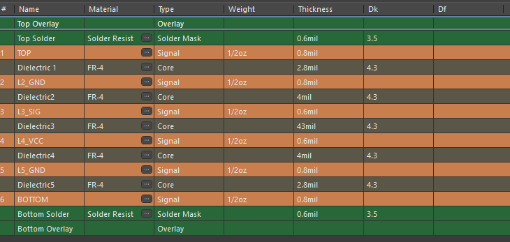
By the end of Phase 2, you should have a simple table that says:
- Interface → target single-ended and differential impedance
- Layers where those nets are allowed to live
- Which plane each of those layers references (GND, PWR)
Example:
- USB 3.x pairs: 90 Ω diff on L2 stripline vs GND
- PCIe pairs: 85 Ω diff on L3 as stripline between GND and PWR
- Clocks: 50 Ω single-ended on top microstrip vs GND
Minimal Pre-Layout SI Check That's Worth Your Time
You do not need a full SI campaign at this stage. You do need one sanity check for the riskiest path.
Pick the Single Worst-Case Channel
- Highest data rate
- Longest distance
- Most connectors / vias in its path
For that one channel:
- Use the fabricator's proposed stackup and trace dimensions
- Use vendor-provided models for driver/receiver (IBIS/IBIS-AMI if available) and connectors (S-parameters if available)
- Build a simple channel model: Driver → trace → via(s) → connector → trace → receiver
Check two things:
- Approximate insertion loss at the Nyquist frequency
- Any obvious discontinuities from long via stubs or bad connector footprints
⚠️ If This Simple Model Already Looks Marginal
It's a clear signal to:
- Shorten the path
- Change material
- Change topology (add retimer)
- Plan for more aggressive via/backdrill strategy
Doing this one check in Phase 2 can prevent an entire generation of "we built it and found out later the physics doesn't work."
What You Can Safely Postpone to Later Phases
You do NOT need in Phase 2:
- Exact length-matching numbers for every bus
- Detailed decoupling placement
- Full 3D EM via models for everything
You DO need:
- Confidence that the chosen stackup and material can support your chosen interfaces with margin
- Agreement with the fab about impedances and which layers are impedance-controlled
- A rough idea which nets are "high-speed class" and must obey those geometries later
Phase 3: Placement
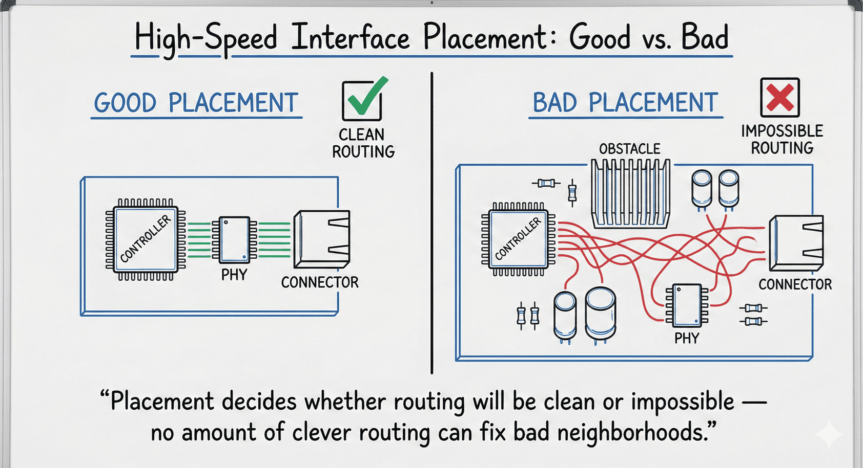
Placement is where you spend (or save) routing and SI effort. By now, schematic and stackup have quietly fixed most of the high-level constraints. Placement decides whether the final channels will be short and clean, or long, tortured, and marginal.
Grouping High-Speed Parts So Routing Isn't Doomed from the Start
High-Speed Interfaces Want Tight, Direct Neighborhoods
- Place the controller/SoC/FPGA, its PHY/SerDes, and the connector as a compact cluster with short, direct escape routes
- No "wall of BGAs" between driver and connector
- For DDR: Place memory devices near the controller with fan-out directions and length-matching patterns in mind
Good placement for SI looks like:
- Straight-ish routes with few layer changes
- Predictable return paths under each group
- Clear separation between different noisy domains (power stages vs sensitive analog vs high-speed digital)
Poor placement forces:
- Zig-zag routes that snake around unrelated components
- Multiple unnecessary layer changes just to escape from congested zones
- High-speed routes over plane splits or through noisy areas
Planning Return Paths and PDN Around Critical Interfaces
At placement time, you can still move parts and bulk components to help both SI and PI.
For Each SI-Critical Cluster
- Make sure there is a solid reference plane under the main routes (usually GND)
- Arrange local decoupling: small caps close to high-speed IC power pins, bulk caps nearby but not blocking routes
- Avoid: Large cut-outs or slots under high-speed routes, or squeezing decaps so tightly that they force critical routes into awkward detours
Think of Each Cluster as a Small "SI Island"
- Components and decaps form the island
- Reference planes and return paths form the "water" around it
- Routing later should follow those contours, not fight against them
Red Flags That Mean You Must Go Back and Fix Stackup or Schematic
⚠️ Certain Placement Problems Are Not Fixable with Clever Routing
Red flags:
- The only way to route a high-speed lane is across a large plane split, through a minefield of unrelated BGAs and vias, or through connectors never meant for those speeds
- The PHY and its connector are so far apart that even a straight line consumes most of the allowed channel length
- You need more high-speed layers than your agreed stackup provides
If you see these, the right move is: Revisit stackup, revisit schematic choices, or re-place the major components. It is cheaper to drag placement back a step than to ship a board where the best-case routing is already outside the physical budget.
Phase 4: Routing
By the time you start serious routing, all the important SI decisions should already be made: interfaces and PHYs (Phase 1), stackup and materials (Phase 2), and high-speed component neighborhoods (Phase 3). Routing is where you implement those decisions and find out whether the plan was realistic.
SI Rules That Must Already Be in Your Constraint Manager
If you open the layout and start routing without constraints, you will violate SI rules by accident.
Before Routing Critical Nets, Your Constraint System Should Know
- Net classes for high-speed groups (PCIE_DIFF, USB3_DIFF, DDR_ADDR_CTRL, DDR_DATA)
- For each class: Target trace width and spacing for impedance, allowed layers, clearance to other nets and copper, length and skew rules, allowed via types and maximum via count
At This Point, "Planning for SI" Means Encoding It
Configure constraints so the tool helps you enforce them. If you only configure constraints after routing, it usually shows you a long list of violations that are painful to fix.
What You Can Still Rescue at This Stage
Some problems are still fixable during routing, especially if discovered early:
- Slightly shuffle component orientations to open cleaner channels
- Move or rotate passive parts to avoid blocking differential pair escape routes
- Change layer assignments for certain nets (within the stackup agreed earlier)
- Widen spacing between aggressor and victim nets to reduce crosstalk
- Add stitching vias or small copper changes to improve return paths
For many mid-speed interfaces (100–200 MHz digital, USB 2.0, moderate-length LVDS), good routing can recover a lot of margin assuming stackup is reasonable, parts are placed sensibly, and routing rules are encoded and checked.
What You Cannot Realistically Fix Without a Re-Spin
⚠️ Routing-Time Discoveries That Usually Mean "This Board Is Compromised"
- Critical lanes cannot reach their destination without excessive via count, crossing plane splits with no room for proper return-path stitching, or exceeding length/skew budgets even with tight routing
- The agreed stackup does not allow the needed trace width/spacing for impedance on the layers where you have space to route
- Length-matching constraints require impossible "trombone" patterns due to lack of free space
- Critical lanes must run in parallel to noisy nets for long distances because there is nowhere else for either to go
When you see these patterns, the problem is not your routing skill. It is that SI planning was late in one of the earlier phases.
At that point, the honest options are:
- Accept a higher risk of SI failure (and possibly build a prototype just to learn)
- Go back one step: re-place key components, re-negotiate the stackup, or in extreme cases adjust schematic choices
Where Basic SI Simulation Actually Fits
Many engineers either never simulate or think SI simulation means a full-blown toolchain and weeks of work. For most boards, you only need two simulation touchpoints, and both are simple.
One Pre-Layout Sanity Sim for the Fastest Link
Belongs at: End of Phase 2 – Stackup Planning, before you commit to placement
Pick the single riskiest channel: Highest data rate on the board, and longest path / most connectors / most vias
Set up a minimal model:
- Use the proposed stackup and trace geometry from the fabricator
- Represent the channel as: Driver model → PCB trace segment(s) → Via(s) → Connector model → Receiver model
What to look at:
- Insertion loss vs frequency: Check at least up to the Nyquist frequency. If loss is already close to the maximum allowed by the PHY spec, you know you have no margin
- Gross discontinuities: Big impedance bumps from via stubs or connector transitions
One Post-Layout Channel Check Before Sending Gerbers
Belongs after: Phase 4 – Routing, when critical nets are fully routed but before you hand off final files
Again, focus on the worst-case channels:
- Extract the routed geometry for those nets: trace lengths on each layer, exact via structures, any connectors or AC coupling caps
- Build a post-layout model: Replace the idealized trace segments with the real ones
Check:
- Eye diagram / margin at the intended data rate
- Jitter and noise contributions
- Whether the channel still meets the vendor's recommended loss and reflection budgets
For Many Projects, Two Simple Simulations Are Enough
One pre-layout, one post-layout, focused on one or two channels—this is enough to catch the big mistakes without turning the project into a simulation marathon.
Summary: SI Planning Timeline on One Page
Think of SI as a series of questions that must be answered no later than certain phases:
Phase 0 – Requirements & Risk
- Do we have high-speed interfaces (multi-hundred MHz or multi-Gbps)?
- Are we reusing a known-good topology or doing something new?
- Do we need to budget for engineered stackup, low-loss material, or advanced vias?
Phase 1 – Schematic
- Which interfaces and PHYs are we committing to?
- Are connectors and cables suitable for those speeds?
- Which nets will later need controlled impedance, skew control, or special routing?
Phase 2 – Stackup Planning
- Layer count, material class, and reference plane structure decided
- Target impedances per interface and per layer agreed with the fab
- One pre-layout sanity simulation for the riskiest link if data rates/lengths justify it
Phase 3 – Placement
- High-speed groups (PHY + controller + connector) placed as compact clusters
- Return paths and local decoupling planned around those clusters
- Red flags (impossible channel distances, forced routes over plane splits) caught early
Phase 4 – Routing
- SI rules encoded in constraints (width/spacing, layers, lengths, skew, via types)
- Critical nets routed according to those constraints, not by eye
- One post-layout channel check for the fastest link before releasing Gerbers
The Key Principle
If you routinely find SI problems at bring-up, move each type of decision one phase earlier in your process.
Frequently Asked Questions
Probably not, if all signals are relatively slow (GPIO, I²C, UART, low-speed SPI) and board dimensions are modest with no long external cables for fast digital signals.
You should still keep clocks and edges reasonably short and avoid routing fast edges over plane splits. But you likely don't need engineered stackup or SI simulation.
A common rule of thumb: If edge rates are fast enough that trace lengths are longer than about 1/6 of the edge distance, treat the traces as transmission lines.
Practically, anything in the hundreds of MHz and above, especially with longer runs or off-board connectors, deserves controlled impedance.
Definitely pay attention once you have: USB 3.x, PCIe, HDMI/DP, multi-Gigabit Ethernet, MIPI, or similar.
If you are using the same stackup, with similar board size and connectors, and following the layout guide closely, you may not need to simulate for the first revision.
However, if you change board size significantly, material class, connector topology, or channel length, then a simple pre-layout and/or post-layout sim for the riskiest link is cheap insurance.
That can mean you genuinely had enough margin, or the prototype works in your lab but is close to the edge and may fail under temperature/voltage extremes, production variation, EMC testing, or field conditions.
If the product is low volume and not safety-critical, you may accept this. For higher volume or long-lived products, it is better to use that first prototype to calibrate your understanding and tighten SI planning on the next design so you rely less on luck.
If you have to pick just one place to start doing better SI planning: Start with stackup planning (Phase 2).
A realistic, well-planned stackup makes routing easier, improves return paths automatically, and gives you predictable impedance and loss.
Once stackup is under control, the next most impactful phase is placement of high-speed components.
Want to Learn More About PCB Design Best Practices?
Check our other blogs where we share practical PCB design insights, automation techniques, and real-world case studies from projects using AI-powered PCB tools.
Visit Blogs Request Technical Discussion