
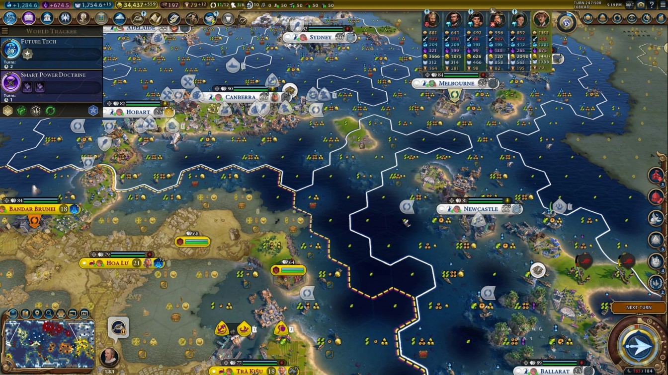
The Thesis: Your Board as a Living Strategy Map
Treat your circuit board as a strategic battlefield where you place "units" (components), allocate scarce resources (area, layers, power), and maintain robust "supply lines" (interconnects and return paths). Success depends on mastering three distinct but interconnected strategic dimensions:
- Chess-like tactics: Precise positioning and thinking several moves ahead
- Civilization-style strategy: Infrastructure building and long-term resource planning
- StarCraft execution: High-tempo optimization under multiple competing constraints

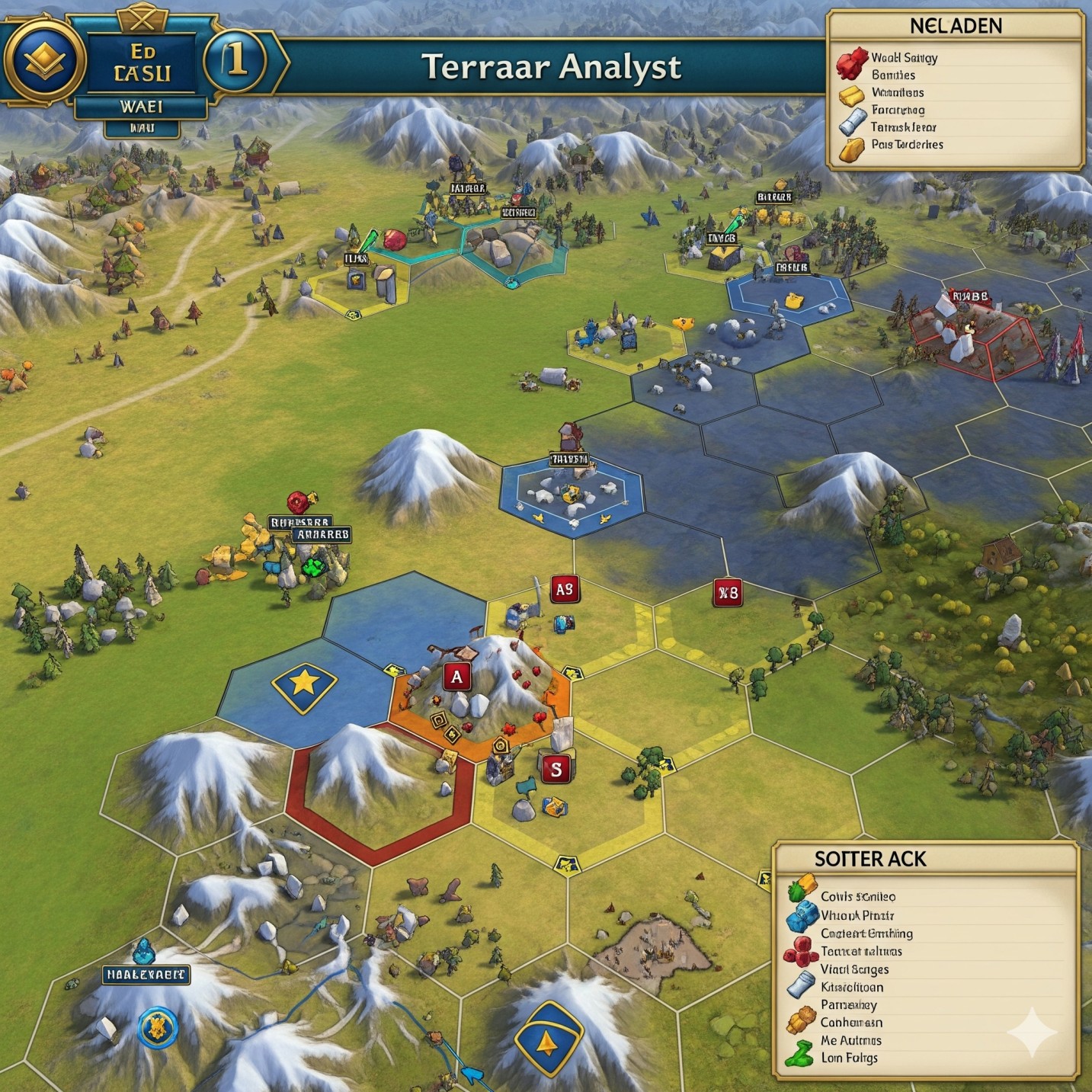
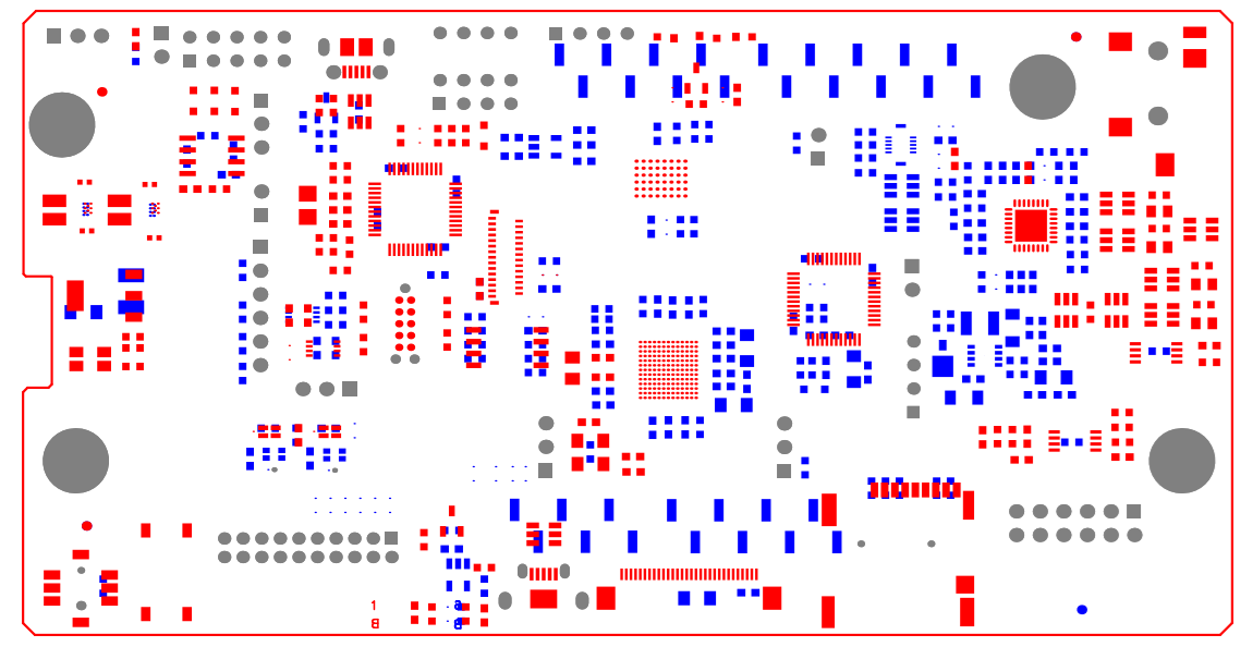
The Board Is Your Map: Terrain, Chokepoints, and Zoning
Before a single trace is routed, your blank board already has "terrain" that determines strategic possibilities:
Understanding Your Strategic Terrain
- Edges: I/O shorelines and harbors (connectors, antennas, buttons)
- Corners: Easy to defend, easy to jam (EMI risk, tight routing angles)
- Interior: High-value real estate (MCUs/SoCs, memory, clock trees)
- Keep-outs: Mountains and rivers (mounting holes, shields, mechanical constraints)
- Layer stack: The vertical dimension (bridges and tunnels via vias)
Like any good strategist, you want defined zones: RF, power, high-speed digital, sensitive analog, and noisy switching kept apart with deliberate corridors for movement (signals) and supply (power/ground).
Component Placement = Unit Positioning
Chess: Protect Your King and Control the Center
Chess analogy: You castle early (protect the king) and centralize your pieces. On PCBs, you secure clocks and power first, then centralize the CPU/MCU with shortest paths to time-critical partners (memory, PHYs).
StarCraft: Army Composition and Concaves
StarCraft analogy: Army composition and concaves matter. On PCBs, component clusters (MCU + RAM + decoupling) must form strong local synergies, with good "concaves" for routing fan-outs and return currents.
Civilization: City Placement on Resources
Civilization analogy: City placement on resources dictates your tech and economy. On PCBs, place on constraints: connectors at edges, crystals close to ICs, high-speed pairs with clean escape routes, sensors at the periphery.
🎯 Practical Placement Heuristics
Anchor first: Lock connectors, mechanicals, antennas, then CPUs/PHYs. Don't fight physics or mechanics—exploit them.
Short, straight, symmetric: Clock and high-speed routes want minimal length, minimal skew, and symmetric geometry.
Localize noise & heat: Keep switching power and hot parts together with thermal relief and guard traces/shields where needed.
Reserve corridors: Leave predictable escape channels from fine-pitch BGAs and dense headers before filling in passives.
Resource Management: The Board's Economy
Like managing minerals & gas (StarCraft) or food/production/gold (Civilization), PCB work is resource budgeting under pressure:
🎮 Gaming Resource Types
- Territory: Map control and expansion
- Economy: Resource generation and collection
- Infrastructure: Buildings and supply lines
- Military: Unit production and positioning
- Technology: Research and advancement
🔧 PCB Resource Types
- Area budget: Every square millimeter is a tile
- Layer count: More layers = more infrastructure, higher cost
- Power budget: VRM topology, copper width, plane integrity
- Via budget: Bridges/tunnels with inductance and cost
- Manufacturing budget: DFM rules and process constraints
🎯 Strategic Decision: Expand or Tech?
Expand = add a layer (more routing freedom, cost ↑)
Tech = improve placement/constraints (more thinking now, cost ↓)
You win by teching first (strong placement & rules) and expanding only when the ROI is clear.
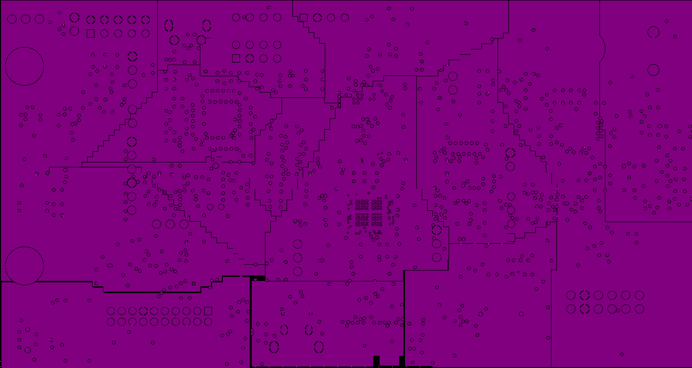
Interconnections = Supply Lines
Civilization's trade routes and StarCraft's supply chains are your traces + returns + planes. Just as armies need secure supply lines, your signals need clean return paths and robust power distribution.
🎯 Supply Line Rules of Thumb
Two-hop rule: Any fast net should find a clean return within two nearby vias or one uninterrupted plane transition.
Never cross a split: With a high-speed net; if forced, provide stitching vias to preserve the return path.
Keep sensitive analog behind "mountains": Guard traces, ground moats, and physical distance.
Gaming Supply Lines
- Trade routes connecting cities (Civilization)
- Pylon power fields (StarCraft Protoss)
- Resource transport networks
- Vulnerable chokepoints requiring protection
PCB Supply Lines
- Signal traces with paired return paths
- Power distribution networks and planes
- Via stitching for plane continuity
- Chokepoints at vias and layer transitions
Multi-Objective Optimization: The Pareto Game
You're balancing cost, performance, manufacturability, reliability, and schedule. There is no single optimum; there's a Pareto frontier of trade-offs.
Strategic Trade-offs
- Cost vs Performance: 4-layer can work, but 6-layer might crush EMI risk
- Density vs Yield: Microvias route miracles, but yield shrinks
- Thermal vs EMI: Copper pours help thermals but alter impedance
Make Trade-offs Explicit
- Define weighted goals (40% performance, 35% cost, 25% schedule)
- Maintain a risk log (EMI, timing margin, via counts)
- Keep multiple stackup options for quick comparison
Long-Term Planning: Openings, Midgame, Endgame
The Three Phases of PCB Strategy
Openings (Architecture & Placement)
Choose the "opening book": reference designs, vendor app notes, and known-good patterns (DDR topologies, Ethernet magnetics). Lock in zones, keep-outs, fan-out strategies, and PDN concept.
Midgame (Routing & Constraint Closure)
Execute with discipline: length/skew rules, layer assignments, via budgets, impedance checks as you go. Don't push problems forward—fix chokepoints when you see them.
Endgame (Verification & DFM)
Like a chess endgame, small errors decide the match. Run comprehensive verification: DRC, ERC, SI checks, PDN analysis, thermal simulations, and manufacturing reviews.
Tactics vs Strategy: APM and CPM
Like StarCraft players who balance Actions Per Minute (APM) with strategic thinking, PCB designers must balance execution speed with strategic planning.
Tactics (APM - Actions Per Minute)
- Push/pull routing adjustments
- Neck-downs and layer swaps
- Via stitching and teardrops
- Fast hands save hours
Strategy (CPM - Critical Path Method)
- Identify long poles (stackup, BGA escape, PDN)
- Attack critical constraints first
- Parallelize routine tasks
- Slow down to set rules; speed up to execute
⚠️ Warning: High APM Can Mask Weak Strategy
Blunders happen when high-speed execution masks weak strategic thinking. Take time to establish solid rules and constraints, then execute them efficiently.
Fog of War: Managing Requirements and Uncertainty
Real projects start with partial specifications, just like strategy games where you can't see the entire map initially. Reduce the fog early through smart reconnaissance:
🎯 Reducing Design Uncertainty
Run quick feasibility sketches of worst-case nets (DDR escape, USB3 lanes)
Prototype stackups with your fab early and lock impedances and materials
Budget risk and plan margins (common-mode chokes, RC snubbers, spare series resistors)
AI and Automation: From Opening Books to Strategic Assistance
Just as chess engines mix policy (what's promising) and search (what actually works), modern PCB workflows benefit from intelligent assistance that doesn't replace strategic thinking—it amplifies it.
Traditional Manual Approach
- Like playing StarCraft without hotkeys
- Every action requires individual attention
- Limited by human processing speed
- Vulnerable to fatigue and oversight
Automation-Enhanced Design
- Like having perfect macro execution
- Focus on strategy while automation handles implementation
- Rapid exploration of design alternatives
- Consistent execution of design rules
🎮 The Strategic Partnership
You don't need full autonomy to win—decision support that highlights congestion, skew risks, and PDN weak spots already pays dividends. The strategy remains human; the execution becomes superhuman.
Battle-Tested Checklists
Like pro gamers who use consistent build orders and strategic checklists, successful PCB designers rely on proven methodologies:
🚀 Before Routing
- Anchors fixed (connectors, antennas, holes, shields)
- Zones drawn (RF / power / digital / analog)
- Fan-out corridors reserved for dense parts
- Draft stackup & impedances confirmed with fab
⚡ During Routing
- High-speed nets first; return paths continuous
- Differential pairs length/skew tracked continuously
- PDN via-stitching and decap proximity verified
- Chokepoints removed early; don't defer
✅ Sign-off
- DRC/ERC clean; controlled-impedance audit
- SI spot-checks on top 5 nets; PDN impedance curve inspected
- Thermal review of top 5 hotspots
- Test-point coverage & assembly notes validated
- BOM alternates for risk parts
Win the Campaign, Not Just the Battle
Like any great strategy game campaign, success in PCB design comes from smart openings, stable economies, resilient supply lines, and disciplined endgames. Treat your layout as a strategic map: every placement is a positional choice, every trace a logistical decision, every rule a doctrine.
When you think like a grand strategist—and execute like a skilled tactician—you ship boards that win on performance, cost, manufacturability, and time.
Ready to Master the Ultimate Strategy Game?
Whether you're a strategy game enthusiast discovering the tactical depth of PCB design, or an engineer looking to level up your strategic thinking, the principles remain the same: master your terrain, position your pieces wisely, manage resources efficiently, and execute with precision.
Start Your Campaign Learn the Advanced Strategies