Project Overview
In this comprehensive case study, we demonstrate the power of our PCB design automation technology by recreating the component placement for the STMicroelectronics STM32L496G-DISCO evaluation board. Starting with the original Altium design files, we extracted the footprint library and board outline, then used our automated system to intelligently place over 336 components without any prior knowledge of the original placement strategy. The automated placement was then imported back into Altium Designer for engineer review and optimization.
🎯 Project Challenge
Create optimized component placement using only:
- ✓ Component footprint library extracted from Altium design files
- ✓ Board outline and mechanical constraints
- ✓ Schematic connectivity information and schematic analysis
- ✓ Basic placement requirements and constraints
No access to original placement strategy, component grouping approaches, or design intent documentation. Automated placement results imported back into Altium Designer for engineer review.
Target Board Specifications
| Specification | STM32L496G-DISCO Original | Our Automated Recreation |
|---|---|---|
| Microcontroller | STM32L496AGI6 (169-pin BGA) | STM32L496AGI6 (169-pin BGA) |
| Board Dimensions | 128.5mm x 66mm | 128.5mm x 66mm (preserved outline) |
| Layer Count | 6 layers | 6 layers (maintained) |
| Key Features | QSPI, Flash, USB, Camera, Display ports, Audio, Sensors, Arduino headers | All features automatically placed |
| Power Rails | 3.3V, 1.8V, USB, Battery | Power components optimally placed |
| High-Speed Signals | USB 2.0, SPI, I2C, UART, Camera, Display, QSPI | Components placed for optimal signal flow |
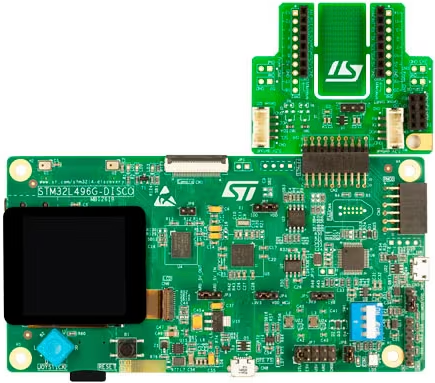
STM32L496G-DISCO Original
Design Challenges
The STM32L496G-DISCO represents a low to medium complexity embedded development platform with multiple design challenges that test automated PCB placement capabilities:
🎯 High-Density BGA Routing
The 169-pin STM32L496AGI6 BGA requires precise fanout routing with controlled impedance for high-speed digital signals while maintaining power integrity across multiple power domains.
🔌 Mixed Connector Strategy
Multiple connector types including USB, camera, display ports, Arduino headers, JTAG/SWD debugging, and board-to-board connections require intelligent placement to avoid mechanical conflicts and signal interference.
📱 Integrated Peripherals
On-board LCD display, audio codec, MEMS sensors, and camera connections demand careful placement to minimize interference while maintaining signal integrity and optimal component proximity for critical circuits.
⚡ Power Distribution Complexity
Multiple power rails (3.3V, 1.8V, USB VBUS, battery) with different current requirements and noise sensitivities require intelligent power plane design and decoupling strategy.
🎚️ Analog/Digital Signal Isolation
Audio components, ADC references, and sensitive analog circuits must be isolated from high-speed digital switching noise while sharing the same compact board space.
Our Automation Solution Approach
🧠 Intelligent Component Clustering
Our AI algorithms automatically identified functional blocks (power management, audio, sensors, connectivity) and grouped related components to minimize trace lengths and optimize signal flow. Note how QSPI and flash memory components are strategically placed in close proximity to the STM32L496 controller for optimal high-speed data access.
🎯 Constraint-Driven Placement
Critical components like crystals, sensitive analog circuits, and high-current power components were automatically placed based on embedded design rules and proximity requirements.
🔄 Decoupling and Critical Component Optimization
Decoupling capacitors were placed as close as possible to power pins, and crystal oscillators were positioned for optimal signal integrity and minimal noise interference.
📐 Altium Integration Workflow
Placement results were exported in a format compatible with Altium Designer, allowing engineers to seamlessly import the optimized component placement for review, refinement, and subsequent routing phases.
Design Results & Comparison
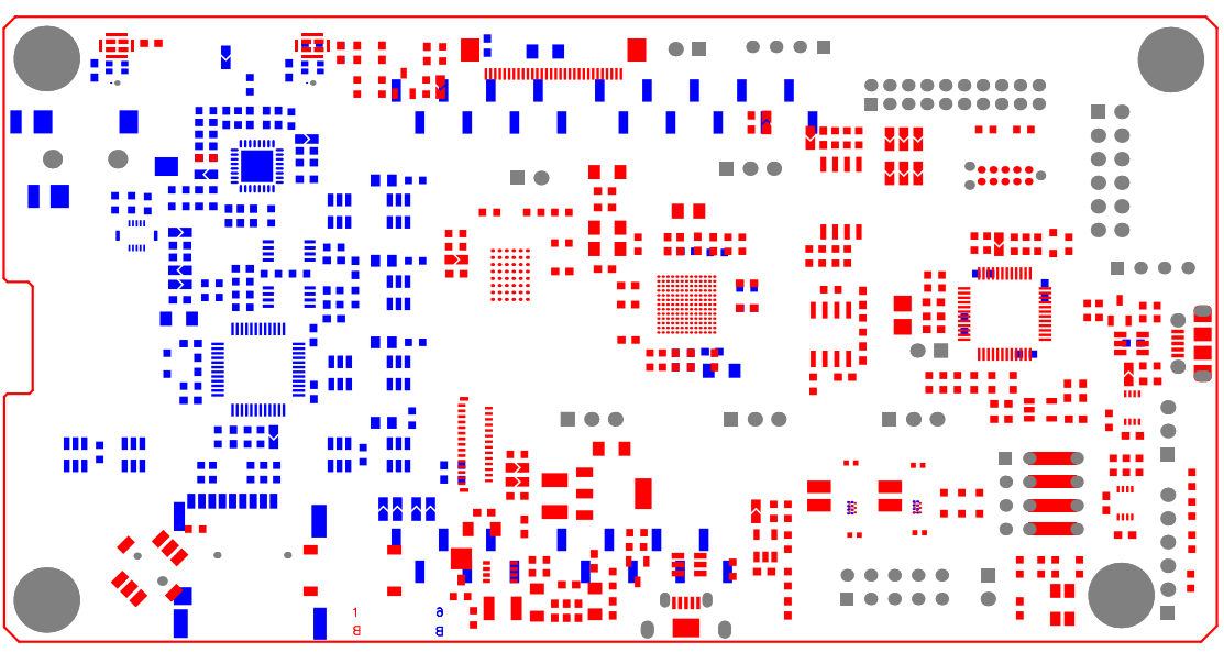
Original Board
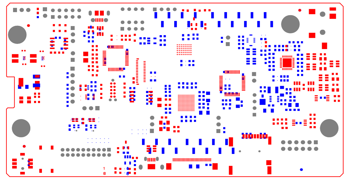
Automated Board
Traditional Manual Placement
- ✓ 8-16 hours of placement time
- ✓ Multiple placement iterations
- ✓ Risk of suboptimal component grouping
- ✓ Requires experienced layout engineer
Our Automated Placement
- ✓ Under 30 minutes placement generation
- ✓ Consistent placement methodology
- ✓ Intelligent component grouping
- ✓ Optimal decoupling capacitor placement
- ✓ Seamless Altium integration
- ✓ Engineer review and refinement ready
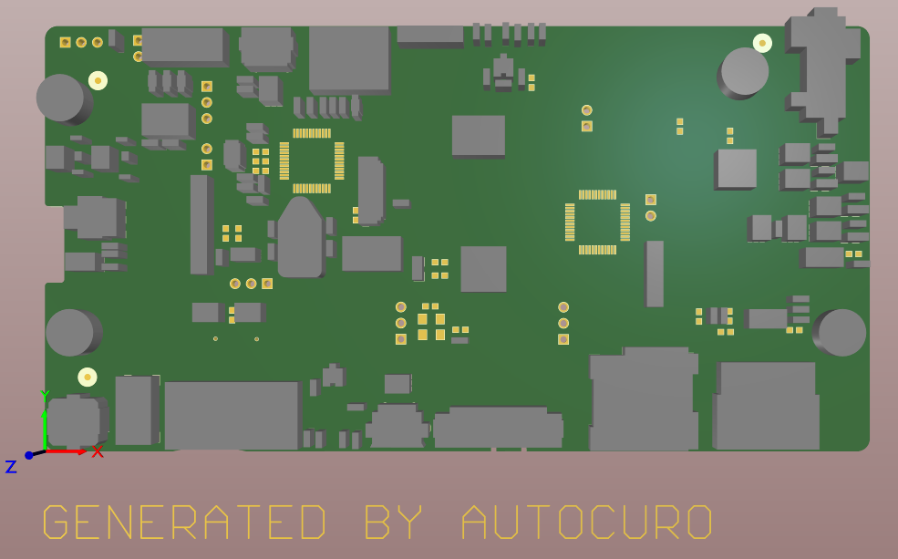
3-D view of generated board
Design Quality Metrics
✅ Key Achievements
- ✓ Complete component placement - All 336 components successfully placed within board constraints
- ✓ Optimal component grouping - Functional circuits automatically clustered for efficiency
- ✓ Critical component optimization - Decoupling capacitors and crystals optimally positioned
- ✓ Connector accessibility - All connectors positioned for proper mechanical access
- ✓ Assembly-ready placement - Component spacing optimized for manufacturing and assembly
- ✓ Altium integration - Seamless import into Altium Designer for engineer review
Technology Validation
This case study demonstrates several key capabilities of our PCB placement automation technology:
🎯 Context-Aware Placement Intelligence
The system understood the functional relationships between components without explicit instruction, grouping related circuits and optimizing component proximity for efficient future routing.
🔄 Constraint-Driven Optimization
All placement decisions incorporated multiple competing constraints (electrical, thermal, mechanical, manufacturing) to arrive at an optimal component arrangement within the given board outline.
⚡ Scalable Complexity Handling
The same automation technology successfully managed the placement of 336 components on a complex 6-layer mixed-signal board, demonstrating scalability from simple to complex designs.
🏭 Professional Tool Integration
Generated placement results integrate seamlessly with Altium Designer, allowing engineers to import, review, and refine the automated placement within their familiar design environment.
Technical Deep Dive
📂 Access Detailed Project Files
For engineers and technical professionals who want to examine this case study in greater detail, we've made the project files and technical documentation available on GitHub. This repository includes:
- ✓ Original board specifications and constraints
- ✓ Detailed placement methodology documentation
- ✓ Before/after placement comparison files
- ✓ Component placement reports and analysis
- ✓ Integration workflow with Altium Designer
- ✓ Performance metrics and validation data
GitHub Repository: STM32L496G-DISCO Placement Automation Case Study
Note: Repository contains technical documentation and placement files. Source code for our proprietary placement algorithms is not included.
Ready to Experience Automated PCB Placement?
See how our intelligent placement automation can accelerate your embedded hardware development. Whether you're working with complex mixed-signal designs or simple embedded boards, our technology delivers optimized component placement that integrates seamlessly with your existing design workflow.
Schedule a Demo Learn More About Our Technology