
Quick Navigation
What Is a PCB Stackup?
A PCB stackup defines the physical layer structure of your board: the number of copper layers, the dielectric materials between them, and the thickness of each layer. It is one of the earliest design decisions you make and one of the hardest to change later. The stackup affects trace impedance, signal integrity, power distribution, EMI behaviour, and fabrication cost — all at once.
Getting the stackup right before routing begins saves significant rework. Changing it after differential pairs are routed, or after impedance-controlled traces are placed, typically means re-running your impedance calculations and adjusting trace widths across the board.
Stackup Decisions That Affect Everything Downstream
- Layer count determines routing density and return path options
- Dielectric material sets your achievable impedance range and loss budget
- Layer arrangement determines where signal, ground, and power planes sit
- Dielectric thickness between signal and reference layers controls trace impedance
- Material Tg (glass transition temperature) affects soldering and thermal reliability
How Many Layers Do You Actually Need?
Layer count is driven by routing density, the presence of controlled-impedance signals, power plane requirements, and EMI shielding needs. More layers add cost and lead time; too few layers can make a design unroutable or force compromises on signal integrity.
Layer Count Decision Guide
| Layer Count | Typical Use Case | Key Considerations |
|---|---|---|
| 2-layer | Simple digital, power supplies, low-speed microcontroller boards | No dedicated ground plane; controlled impedance is difficult; suitable for designs with no high-speed interfaces |
| 4-layer | Most general-purpose digital designs: USB, Ethernet, SPI, I2C, moderate-speed processors | Dedicated ground and power planes; supports controlled impedance on outer layers; most cost-effective entry point for signal integrity |
| 6-layer | Designs with multiple high-speed interfaces (USB 3.x, PCIe Gen1/2, DDR4, HDMI), BGAs, or significant routing congestion | Two inner signal layers plus dedicated reference planes; enables stripline routing; better EMI shielding |
| 8-layer and above | Complex SoC designs, PCIe Gen3/4/5, DDR5, high-density BGA, server/networking boards | Multiple reference planes allow shielded stripline; essential for high-loss-budget protocols; significant cost increase |
💡 Starting Point Rule
If your design has any USB 3.x, PCIe, DDR4, or HDMI, start with 6 layers as your baseline. A 4-layer board can work for USB 2.0, Gigabit Ethernet, and moderate-speed processors, but only if your routing density permits dedicated inner planes. Two-layer boards are generally not suitable for any controlled-impedance requirement.
When to Go from 4 to 6 Layers
- Multiple high-speed interfaces: If you have more than one high-speed interface (e.g., USB 3.0 and PCIe on the same board), 6 layers gives you dedicated routing layers for each without sharing reference planes
- BGA components: Dense BGAs often require an inner signal layer for breakout routing that cannot be achieved on outer layers alone
- Mixed signal designs: Separating analog and digital ground references becomes cleaner with additional layers
- EMI requirements: Designs subject to strict radiated emissions limits benefit from the additional shielding that inner stripline layers provide
- Routing congestion: If your 4-layer route is above roughly 70–80% completion, consider moving to 6 layers rather than compromising signal paths
Choosing the Right PCB Material
PCB material selection is mostly a question of signal loss budget, data rate, trace length, operating temperature, and cost. For most digital designs, the choice is between standard FR-4 and its enhanced variants. RF and high-speed serial designs require more careful consideration.
The two electrical properties that matter most are the dielectric constant (Dk, also written as εr) and the dissipation factor (Df, also written as loss tangent). Dk affects trace impedance and propagation velocity; Df determines how much signal energy is absorbed by the dielectric as frequency increases. Both vary across frequency, and better materials have more stable, lower values of each.
A common simplification is to frame material choice purely around frequency ("FR-4 works below X GHz"). In practice, the right question is whether your total insertion loss budget is met — which depends on trace length and data rate together, not frequency alone. A 5 Gbps signal on a 200 mm trace loses far more than the same signal on a 50 mm trace, even at the same nominal frequency content. Always evaluate material against your actual loss budget, not a frequency threshold.
Material Comparison
| Material | Typical Dk (at 1 GHz) | Typical Df (at 1 GHz) | Relative Cost | Best For |
|---|---|---|---|---|
| FR-4 (standard) | ~4.3–4.8 | ~0.020–0.025 | Low | General digital, <1 GHz signals, cost-sensitive designs |
| FR-4 High-Tg (e.g., Tg 170) | ~4.3–4.8 | ~0.020–0.025 | Low–Medium | Same electrical profile as standard FR-4; used where lead-free soldering or elevated operating temperatures are a concern |
| FR408 / FR408HR | ~3.65–3.75 | ~0.009–0.013 | Medium | Mid-to-high-speed designs: USB 3.x, SATA, PCIe Gen1/2, 10G Ethernet; better Dk/Df consistency than FR-4 |
| Megtron 6 (Panasonic) | ~3.4–3.7 | ~0.002–0.004 | High | High-speed server/networking: PCIe Gen4/5, 25G/100G Ethernet, high-layer-count backplanes |
| Rogers 4003C | ~3.55 | ~0.0027 | High | RF and microwave from ~1 GHz; stable Dk across frequency; more processable than PTFE. Not UL 94V-0 rated — designs using 4003C may require system-level compliance handling for flame retardancy certification |
| Rogers 4350B | ~3.48 | ~0.0037 | High | RF and microwave; UL 94V-0 flame retardant rated — required for consumer and commercial products with regulatory compliance requirements (e.g., CE, FCC). Widely used for antenna boards and 5G sub-6 GHz designs |
| PTFE-based (e.g., Rogers RT/duroid 5880) | ~2.2 | ~0.0009 | Very High | High-frequency RF and mmWave above ~10 GHz; demanding to fabricate; not suitable for standard PCB processes |
Material Selection by Application
| Application | Recommended Material | Notes |
|---|---|---|
| General digital / low-speed (<100 MHz) | FR-4 (standard) | Sufficient for most microcontroller, power, and low-speed communication designs |
| USB 2.0, 100M/1G Ethernet, SATA | FR-4 with care, or FR408 | FR-4 is usable with careful stackup; FR408 gives more margin and more consistent impedance |
| USB 3.x, PCIe Gen1/2, 10G Ethernet, DDR4 | FR408 / FR408HR | Lower loss and tighter Dk tolerance are important at these speeds; standard FR-4 may not meet loss budget |
| PCIe Gen4/5, 25G+ Ethernet, DDR5, high-speed backplanes | Megtron 6 | Very low Df is required to meet insertion loss budgets at these data rates; confirm with your fab |
| RF / Microwave (1–10 GHz) | Rogers 4003C or Rogers 4350B | Stable, low-loss dielectric; required for controlled impedance accuracy at RF frequencies |
| mmWave / High-frequency RF (>10 GHz) | PTFE-based (RT/duroid or similar) | Specialist fabrication required; discuss with your fab early; not interchangeable with standard PCB processes |
⚠️ FR-4 at High Speed: Know the Limits
Standard FR-4 has a relatively high and variable Df (~0.020–0.025). Whether this is a problem depends on your trace length and data rate together — a short 50 mm trace at 5 Gbps may pass your loss budget on FR-4, while a 200 mm trace at the same data rate may not. Glass weave skew is a separate concern: the periodic weave pattern of the glass fibre reinforcement can introduce intra-pair skew on differential signals at high data rates. Mitigations include routing traces at a 10–15° angle to the weave axis, or specifying spread-glass or flat-glass laminates from your fabricator. If your design includes traces above ~5 Gbps, verify your insertion loss budget explicitly before committing to FR-4.
Loss Breakdown: Dielectric, Conductor, and Roughness
Total insertion loss on a PCB trace has three main contributors, and their relative importance shifts with frequency:
- Dielectric loss: Caused by the Df of the laminate material. Scales roughly linearly with frequency and trace length. Dominant at higher frequencies — the primary reason to move from FR-4 to FR408 or Megtron 6 for high-speed interfaces
- Conductor loss: Resistive loss in the copper trace. Increases with the square root of frequency (skin effect). Significant at lower frequencies and on thin or narrow traces; at very high frequencies, dielectric loss overtakes it
- Surface roughness loss: As frequency increases, current concentrates on the surface of the conductor (skin depth shrinks). A rough copper surface — common on standard electrodeposited foil — increases the effective path length and raises conductor loss. Low-profile (LP) or very-low-profile (VLP) copper foils reduce this effect and are specified on high-speed laminates such as Megtron 6
When evaluating materials for high-speed designs, look at all three contributors together. Switching to a low-Df laminate while retaining standard-roughness copper foil will recover dielectric loss but not roughness loss — both need to be addressed for the best insertion loss performance at data rates above ~10 Gbps.
Controlled Impedance and the Stackup
Controlled impedance is not a property you dial in on a single trace — it is a result of the interaction between trace geometry (width, thickness), the dielectric constant of the surrounding material, and the distance to the nearest reference plane. All three are determined by the stackup. This is why stackup selection and impedance planning must happen together.
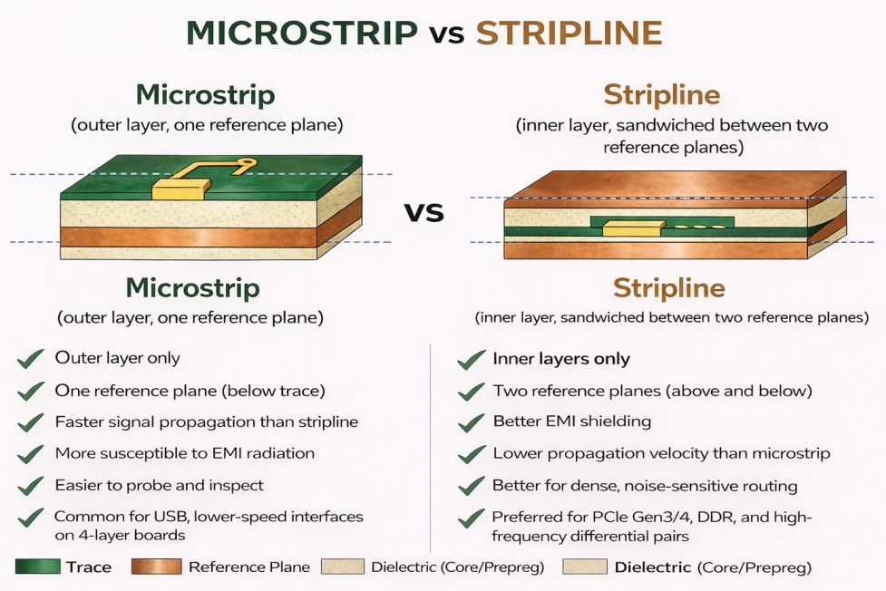
Microstrip vs Stripline
The two most common controlled-impedance structures are microstrip (trace on an outer layer, one reference plane below) and stripline (trace on an inner layer, reference planes above and below). Each has distinct characteristics:
Microstrip
- Outer layer only
- One reference plane (below trace)
- Faster signal propagation than stripline
- More susceptible to EMI radiation
- Easier to probe and inspect
- Common for USB, lower-speed interfaces on 4-layer boards
Stripline
- Inner layers only
- Two reference planes (above and below)
- Better EMI shielding
- Lower propagation velocity than microstrip
- Better for dense, noise-sensitive routing
- Preferred for PCIe Gen3/4, DDR, and high-frequency differential pairs
How Stackup Parameters Affect Impedance
The relationships are straightforward in direction, even if the exact values require a field solver to compute accurately:
- Wider trace → lower impedance: More copper area relative to the reference plane reduces impedance
- Thicker dielectric (greater distance to reference plane) → higher impedance: More separation between trace and plane increases impedance
- Higher Dk material → lower impedance: A higher dielectric constant concentrates the electric field, reducing impedance
- Tighter intra-pair gap (differential) → lower differential impedance: Closer coupling between P and N lowers Zdiff
Typical Controlled Impedance Targets by Interface
| Interface | Single-ended Z0 | Differential Zdiff | Tolerance |
|---|---|---|---|
| USB 2.0 | — | 90Ω | ±15% |
| USB 3.x | — | 90Ω† | ±7% |
| Ethernet (all speeds) | — | 100Ω | ±5–10% |
| PCIe Gen1/2 | — | 85Ω | ±7% |
| PCIe Gen3/4 | — | 85Ω | ±5% |
| DDR4 (clock, DQS) | 40–50Ω* | 100Ω | ±10% |
| LVDS | — | 100Ω | ±10% |
| RF microstrip (general) | 50Ω | — | ±5% |
Always derive the actual trace width and gap from your fabricator's stackup using a field solver. These values are starting points, not universal rules.
* DDR4 single-ended impedance: generic values of 40–50Ω are a starting point only. The correct target is controller-dependent — your SoC or CPU hardware design guide specifies the required impedance and tolerance, and that document takes precedence over any generic recommendation. Always obtain and follow the platform-specific guide before finalising trace widths.
† USB 3.x: the USB-IF specification defines 90Ω ±7% as the standard differential impedance target. This is the correct default. Some processor vendors — notably Intel on certain platforms — specify 85Ω in their hardware design guides for USB 3.x and PCIe lanes. 85Ω is a platform-specific deviation, not a general recommendation. Always check your SoC or host controller's hardware design guide; if it specifies 85Ω, use that. If it does not, use 90Ω.
Return Path Discontinuities
Controlled impedance is only half of the picture. Every signal trace has a return current — and that return current travels in the reference plane directly beneath (or above) the trace, mirroring the signal path. When the return path is interrupted, the signal integrity degrades regardless of how well the trace impedance is controlled. This is one of the most commonly overlooked issues in high-speed PCB stackup design.
For detailed guidance on how this applies to differential pairs specifically, see our guide on differential pair routing guidelines and stackup selection.
- Via layer transitions: When a trace changes layers via a through-hole via, the return current must also find a path to the new reference plane. Without a stitching via placed within 1–2 mm of the signal via, the return current is forced to take a long detour through the plane, radiating EMI and causing impedance discontinuity at the transition point
- Plane splits: A gap or split in the reference plane forces the return current to flow around the gap — potentially across a long path. Routing a high-speed signal over a plane split introduces a significant discontinuity and is one of the most reliable ways to cause EMI failure. If a split is unavoidable, bridge it with a stitching capacitor close to the crossing point
- Reference plane changes: Routing a trace over a layer where the reference plane changes from ground to power (or vice versa) changes the return current's reference. This is manageable if the planes are well-decoupled, but should be avoided for the most sensitive high-speed signals
⚠️ The Return Path Is Part of the Transmission Line
A controlled-impedance trace that crosses a plane split or transitions layers without a stitching via is not a well-behaved transmission line — it is a transmission line with a discontinuity at that point. PCB stackup design rules in most EDA tools cover trace geometry and clearance, but return path continuity is not automatically enforced. It requires deliberate review during layout.
Common Stackup Configurations
The most widely used configurations are 4-layer and 6-layer. Both have well-established layer arrangements that balance routing, signal integrity, and cost.
4-Layer Stackup (Standard)
The most common 4-layer arrangement places signal layers on the outer surfaces with dedicated ground and power planes on the inner layers:
Layer 2: Ground plane
Layer 3: Power plane
Layer 4: Signal (Bottom) — microstrip reference plane above
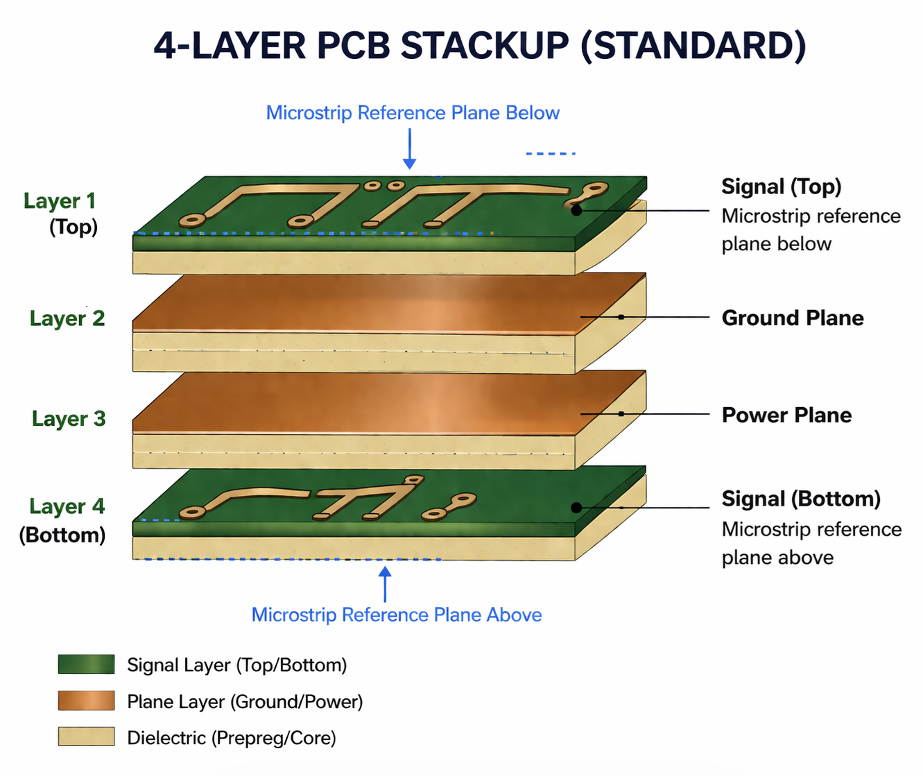
- Both outer signal layers have a reference plane immediately adjacent, which supports controlled impedance on both surfaces
- Ground and power planes are adjacent, which provides natural decoupling capacitance between them
- Suitable for USB 2.0, 100M/1G Ethernet, SPI, I2C, moderate-speed ARM processors on FR-4 or FR408
- Limitation: No inner signal layer; high-density BGAs may be difficult to break out
6-Layer Stackup (High-Speed)
A common EMC-friendly 6-layer arrangement places both inner signal layers between reference planes, ensuring true stripline routing for the inner layers and microstrip on the outer surfaces:
Layer 2: Ground plane
Layer 3: Signal (Inner 1) — Asymmetric stripline (between L2 GND and L4 PWR)
Layer 4: Power plane (or 2nd Ground)
Layer 5: Ground plane
Layer 6: Signal (Bottom) — Microstrip (reference plane above on L5)
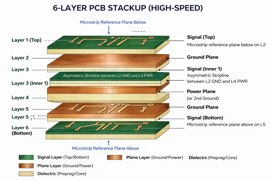
- Layer 3 is a true asymmetric stripline, sandwiched between the Ground plane on L2 and the Power plane on L4 — both act as AC reference planes for signal integrity purposes, provided the power plane is low-impedance and adequately decoupled with bypass capacitors. Without sufficient decoupling, the power plane's AC impedance rises at high frequencies and its effectiveness as a reference degrades
- Both outer signal layers (L1 and L6) are microstrip, each with an immediately adjacent reference plane — L2 for L1, and L5 for L6
- Suitable for USB 3.x, PCIe Gen1/2, DDR4, HDMI, and designs with BGA components
- Important: If you need a second inner signal layer (e.g., L4 or L5), the power plane must be reassigned and the layer arrangement revisited — placing two signal layers adjacent with no reference plane between them will compromise EMI and crosstalk performance significantly
⚠️ A Common 6-Layer Mistake: Unshielded Inner Signal Layers
Placing a signal layer adjacent to another signal layer with no reference plane between them — for example, L5 as signal when L6 is also signal — means L5 is not a true stripline. It will have poor return path continuity, increased crosstalk risk from crossing traces on L6, and is likely to fail radiated emissions requirements. If your routing density requires two adjacent inner signal layers, consult your fab about an 8-layer stackup instead.
⚠️ There Is No Single "Correct" Stackup
The configurations above are common starting points. Your fabricator will have their own standard stackup offerings with specific core and prepreg thicknesses. Always start from your fab's standard stackup, then adjust dielectric thicknesses as needed to hit your impedance targets — do not design a theoretical stackup and then ask a fab to match it exactly, as this adds cost and lead time.
What to Tell Your Fabricator
Clear stackup documentation prevents manufacturing errors and avoids back-and-forth that delays your build. Most fabricators have standard stackup offerings — your job is to specify which requirements are fixed constraints and which are flexible. For a broader pre-layout checklist that covers stackup alongside other design requirements, see our PCB design checklist for layout engineers.
Essential Information to Provide
- Layer count and overall board thickness: e.g., 4-layer, 1.6 mm finished thickness
- Controlled impedance requirements: List each impedance target, its tolerance, the layer it applies to, and which nets or net classes it covers (e.g., "90Ω ±10% differential on Layer 1, nets USB_DP / USB_DM")
- Material specification: Name the material or specify the electrical requirements (Dk, Df) and let the fab propose a material if you have flexibility
- Copper weight per layer: e.g., 1 oz outer, 0.5 oz inner — affects trace resistance and current capacity
- Dielectric thickness constraints: If any layer spacing is fixed (e.g., to achieve a specific impedance), call it out explicitly
- Surface finish: HASL, ENIG, OSP — relevant for solderability, shelf life, and RF performance
Impedance Callout Format
A clear impedance callout on your fabrication drawing removes ambiguity. Include it in a table on the drawing rather than relying on notes in the Gerber files alone:
Controlled impedance — Layer 1 (Top): 90Ω ±10% differential
Trace width: per stackup, ~0.15 mm / gap ~0.18 mm (fab to confirm)
Reference: IPC-2141A
💡 Ask for the Stackup Before You Route
Request your fabricator's standard stackup document — including dielectric thicknesses and material Dk/Df values — before you finalize your impedance trace widths. Running your impedance calculations against the actual fab stackup, rather than a generic model, means your trace widths are correct the first time. Most fabs will provide this on request without charge.
✅ DO
- Start from your fab's standard stackup
- Specify impedance requirements per layer with tolerances
- Confirm material Dk/Df values with the fab before routing
- Include a stackup table in your fabrication drawing
- Specify copper weight per layer
❌ DON'T
- Design a custom stackup and demand the fab match it exactly
- Use generic impedance calculators without the actual fab Dk values
- Leave impedance requirements as informal notes in email
- Assume all FR-4 from different fabs has the same Dk
- Specify impedance without specifying which nets it applies to
Frequently Asked Questions
Want to Know More About How We Use AI with PCB Design?
Check out our comprehensive blog covering AI-assisted PCB design verification across Altium, Cadence, KiCad and other tool series.
Blogs