Project Overview
This case study documents the automated design of a Thunderbolt PCIe Adapter (Thunderboard) using KiCad PCB automation. Rather than marketing claims, we present an honest assessment of what current automation technology can achieve on this board, including the manual refinement still required for production-ready results.
| Specification | Details |
|---|---|
| Design Tool | KiCad 8/9 |
| Board Name | Thunderbolt PCIe Adapter (Thunderboard) — github.com/antmicro/thunderbolt-pcie-adapter |
| Application | Thunderbolt 3 to PCIe x4 Gen 3.0 protocol bridge / adapter |
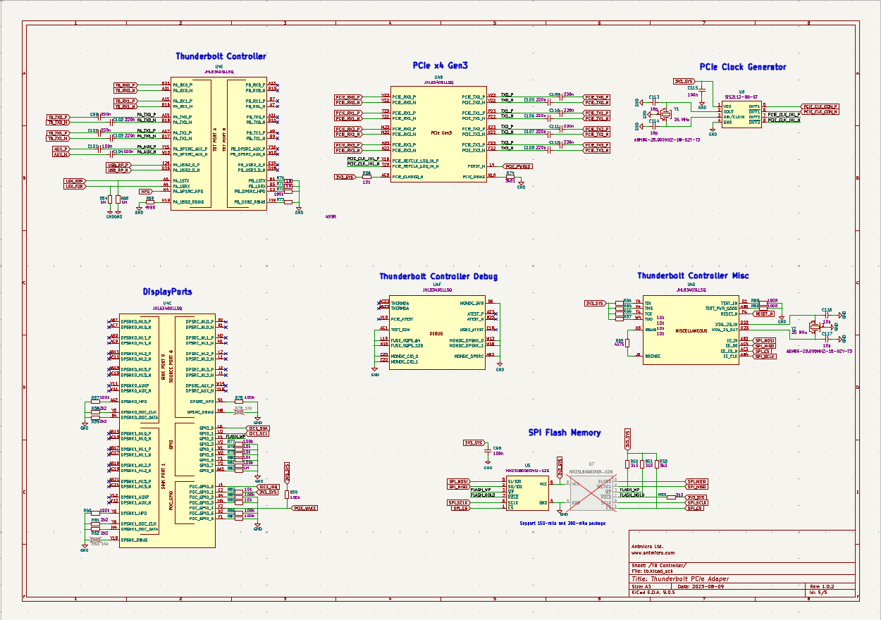
| Core IC | Intel JHL6340SLLSQ — Thunderbolt 3 Controller |
| Board Layers | 6-layer stackup with dedicated signal and power/ground planes |
| Routing Complexity | High — 25 differential traces, 337-pad BGA at 0.65mm pitch, multiple power shapes |
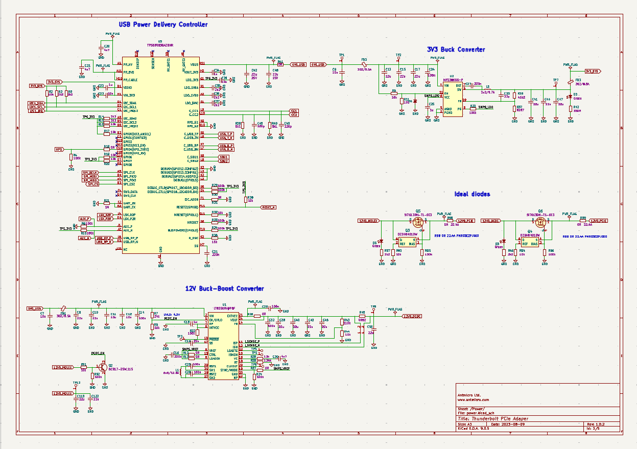
| Key Signals | Thunderbolt 3 differential pairs (USB-C upstream), PCIe x4 Gen 3.0 differential TX/RX lanes, 12V Step-Up DC-DC power rail |
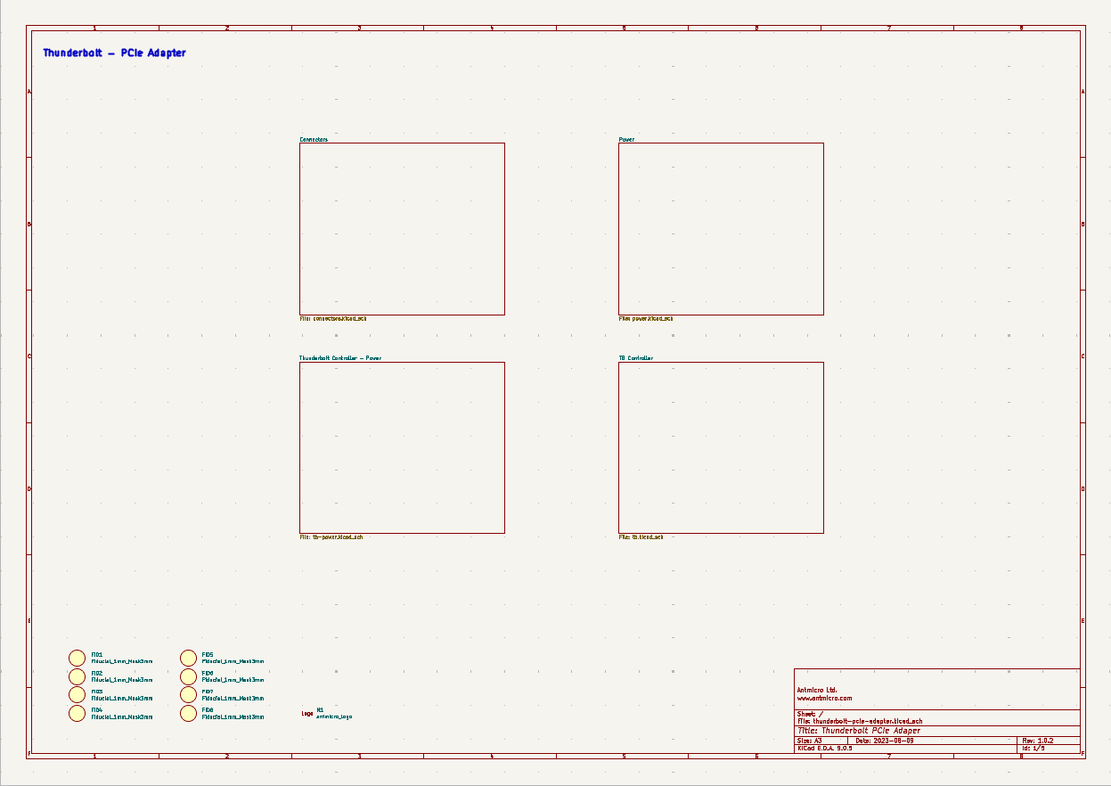
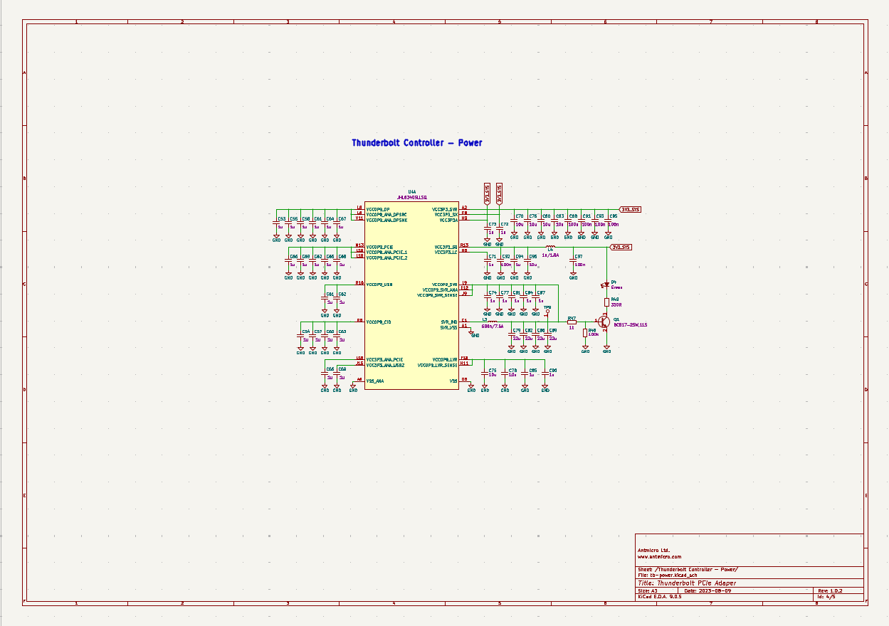
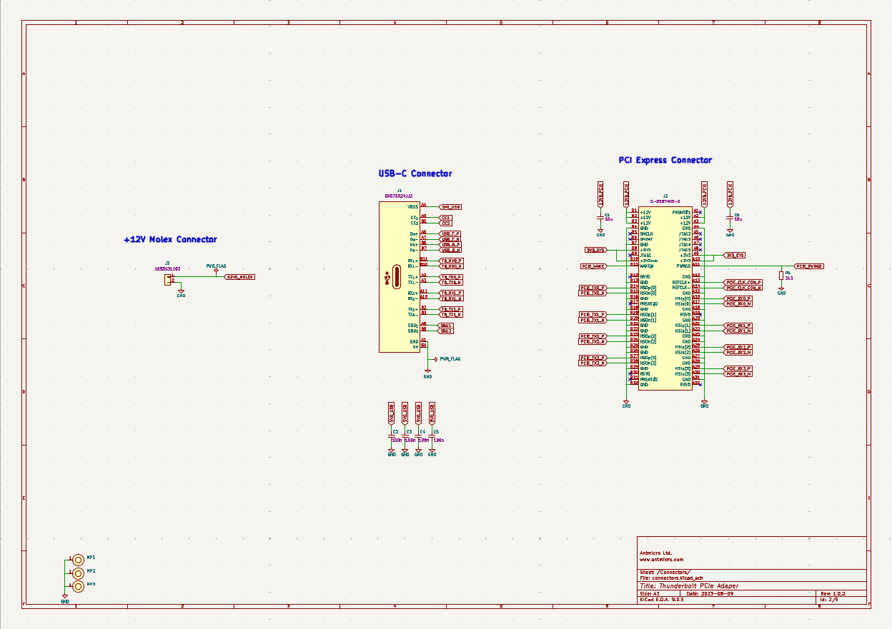
| Schematic Structure | Multi-hierarchy KiCad schematic (5 sheets: top-level, tb, tb-power, power, connectors) |
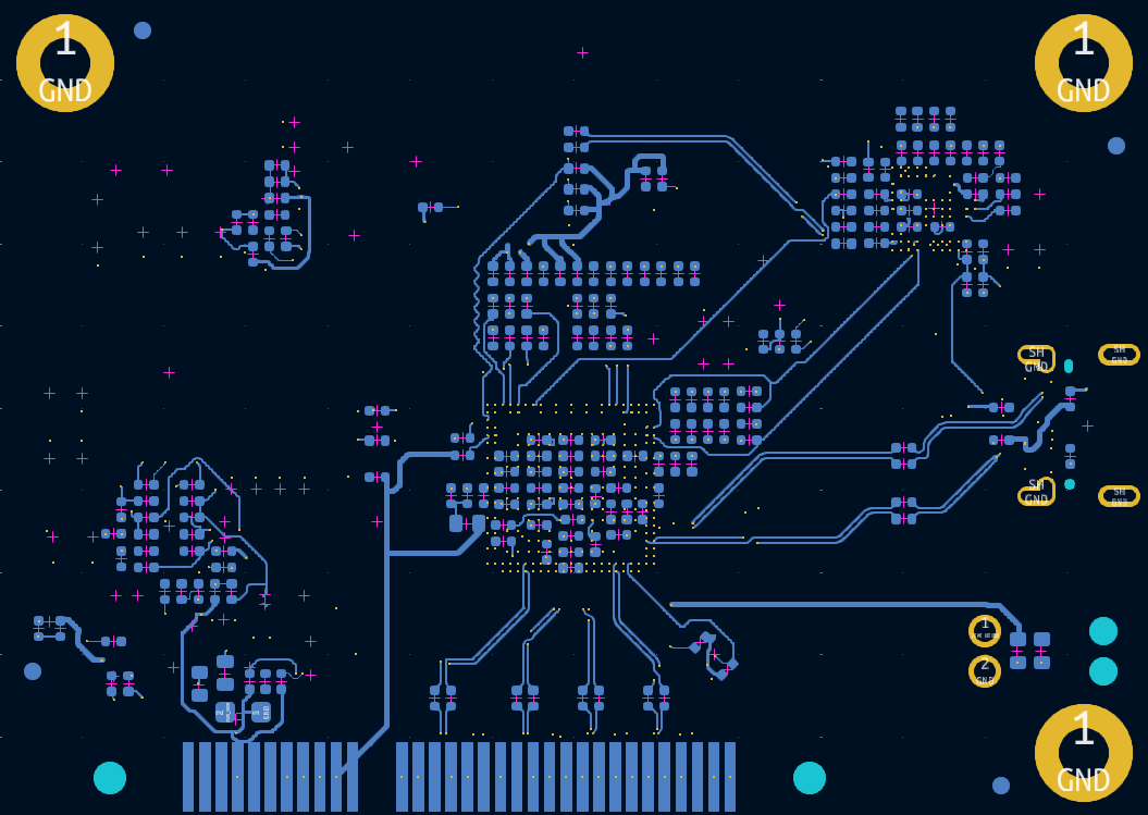
| Autorouting Results | Differential traces routed 22/25, Signal routing 238/242, Number of vias: 607, Power routed traces and planes |
| Compute Requirements | 16 core CPU, 16GB RAM, Windows system |
| Execution Time | 3 hours |
Design Challenge
Here are some key PCB placement and routing challenges:
📍 Multi-Hierarchy Schematic Parsing
The design is organized across five KiCad schematic sheets: a top-level sheet referencing dedicated sub-sheets for the Thunderbolt controller (tb), Thunderbolt power (tb-power), main power supply (power), and connectors. The automation parses this multi-hierarchy structure to extract functional block relationships and net connectivity, which are used to generate design constraints before any placement decisions are made.
⚡ Differential Pair Routing
The board contains 25 differential traces spanning the Thunderbolt 3 upstream interface and the PCIe x4 Gen 3.0 downstream lanes. These pairs require consistent spacing and must be routed with awareness of pairing discipline throughout their full length from source to destination.
🔌 BGA Fanout at 0.65mm Pitch
The Intel JHL6340 Thunderbolt 3 controller is packaged in a 337-pad FC-CSP BGA measuring 10.7×10.7mm with an inner grid pitch of 0.65mm and a perimeter row pitch of 0.46mm. Routing out of this fine-pitch package requires careful via-in-pad placement and layer transition planning to avoid clearance violations while maintaining signal routing continuity. The automated router handles this directly — the engineer does not need to manually configure the escape strategy.
🎯 Power Shape Complexity
The board includes multiple power domains — including a 12V/5V/3.3V rail generated by an on-board Step-Up DC-DC converter to supply PCIe expansion cards. The automation identifies these voltage domains from the schematic hierarchy and generates appropriate power shapes and fanout without requiring manual intervention. The PCB stackup was selected by the automated tool, with clear layer assignments for signal and power routing.
Automation Approach
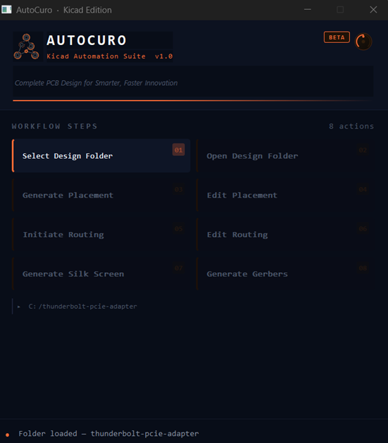
The automation runs locally as a desktop application. The dashboard allows the engineer to select the design folder and run placement, routing, or both steps independently. The design folder must contain the KiCad schematic and board files — the .kicad_sch and .kicad_pcb files.
Schematic-Driven Intelligence
The workflow is structured as eight sequential steps, from folder selection through to Gerber generation. The screenshot below shows the AutoCuro · KiCad Edition dashboard with the thunderbolt-pcie-adapter design loaded and ready to process.
From the schematic hierarchy, the automation identified the Thunderbolt controller block and its surrounding decoupling network, the PCIe connector interface with its four TX/RX differential lane pairs, the Step-Up DC-DC converter and its power distribution, and the crystal oscillator circuit. These functional groupings directly informed the placement strategy.
Schematic Pages
Placement and Routing Control
The automation gives engineers direct control over which steps to run. Pressing Placement generates both component placement and routing in a single pass. Alternatively, pressing Initiate Routing takes the existing placement as-is and generates routing on top of it, without modifying component positions.
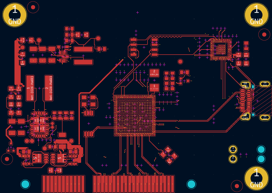
This separation is useful in practice. An engineer can accept the automated placement and route it, replace it with a custom placement and then route, or iterate on placement independently before committing to routing. In this case study, the automated placement was used as a starting point, reviewed, and a revised placement was then used as the basis for the final routed output — demonstrating that the two steps can be decoupled when the design requires it.
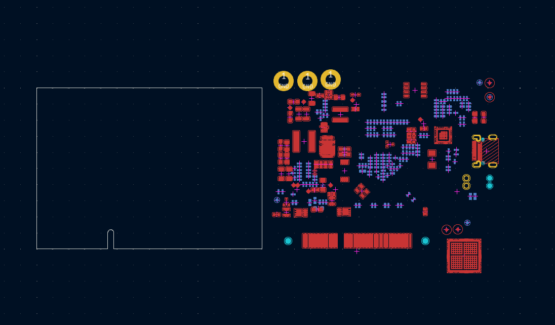
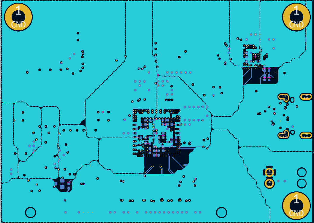
Automated Component Placement
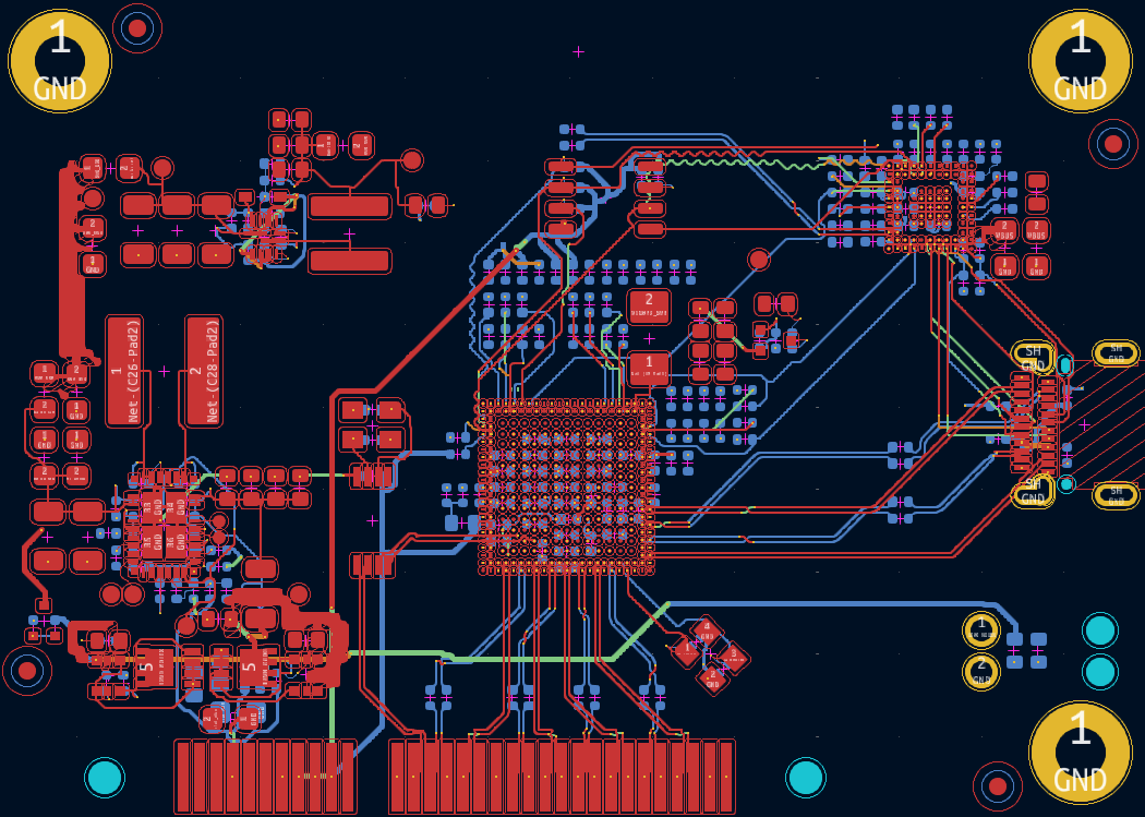
The automated placement produced a complete component arrangement for the Thunderboard, including correct placement of the Intel JHL6340 BGA, the PCIe edge connector, the USB-C Thunderbolt connector, the DC-DC converter, supporting passives, and the crystal oscillator. This is the first board in our case study series where full placement with BGA routing, differential pair routing, and DFA/DFM report generation was demonstrated end-to-end. For the final routed output, the automated placement was reviewed and a revised placement was used — the tool supports running placement and routing as independent steps, which made this workflow straightforward. Placement quality is an ongoing focus area.
Placement Strategy
The automation organized components around the primary routing topology — placing the Thunderbolt controller centrally relative to both the USB-C upstream connector and the PCIe downstream slot, with the power subsystem positioned to support distribution across both interfaces.
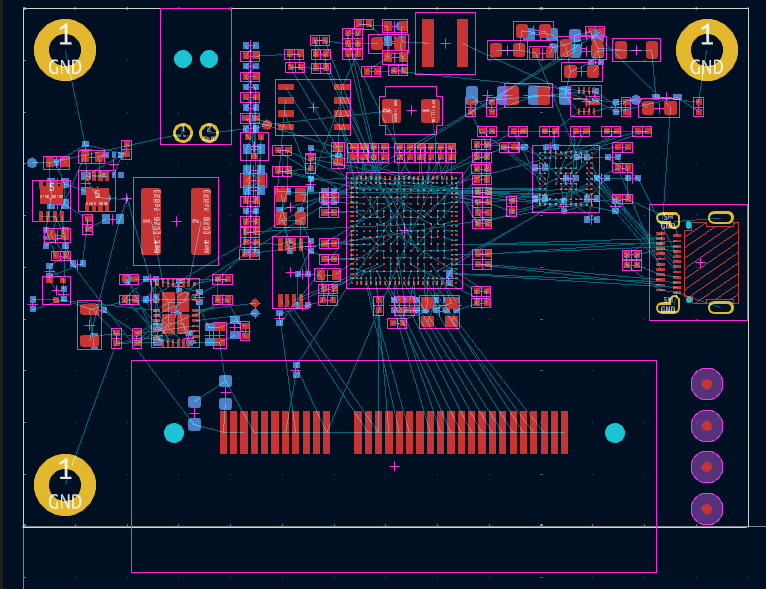
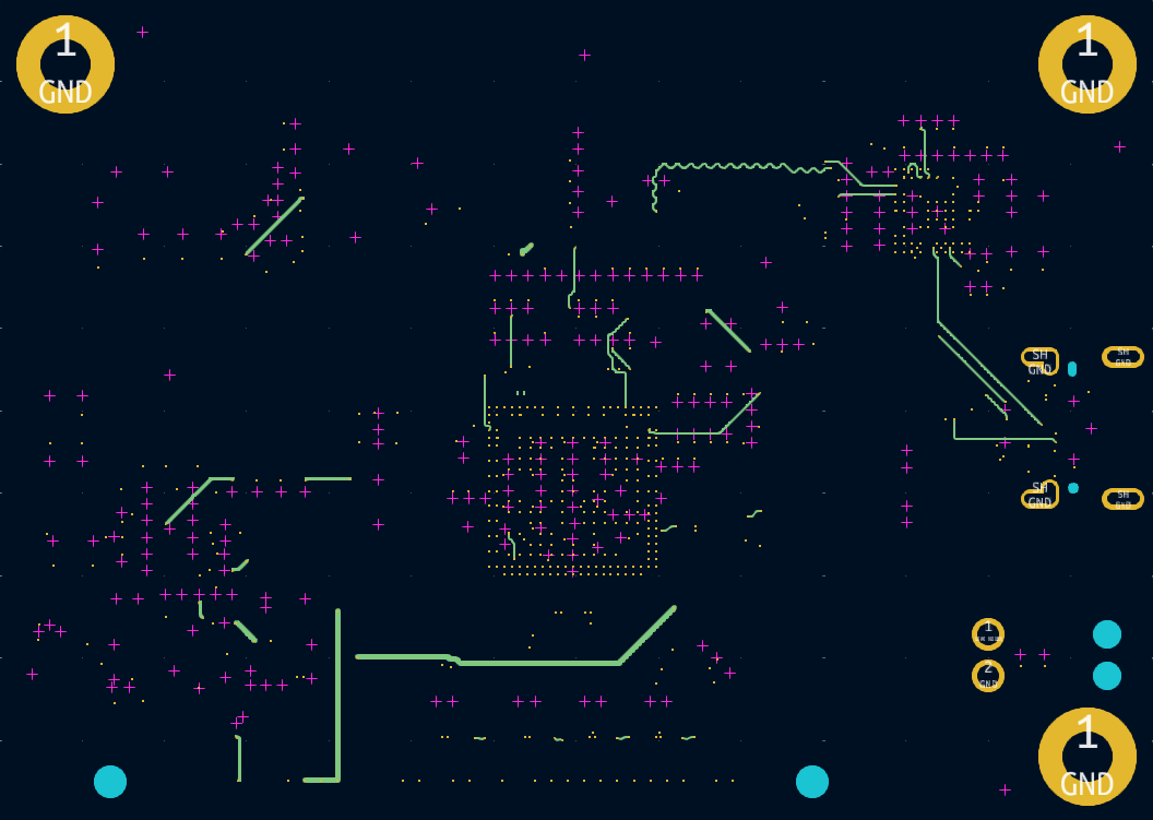
- Original Board: Components unplaced — the Antmicro repository provides the schematic and board outline without a finalized placement, making this a clean baseline for automation input
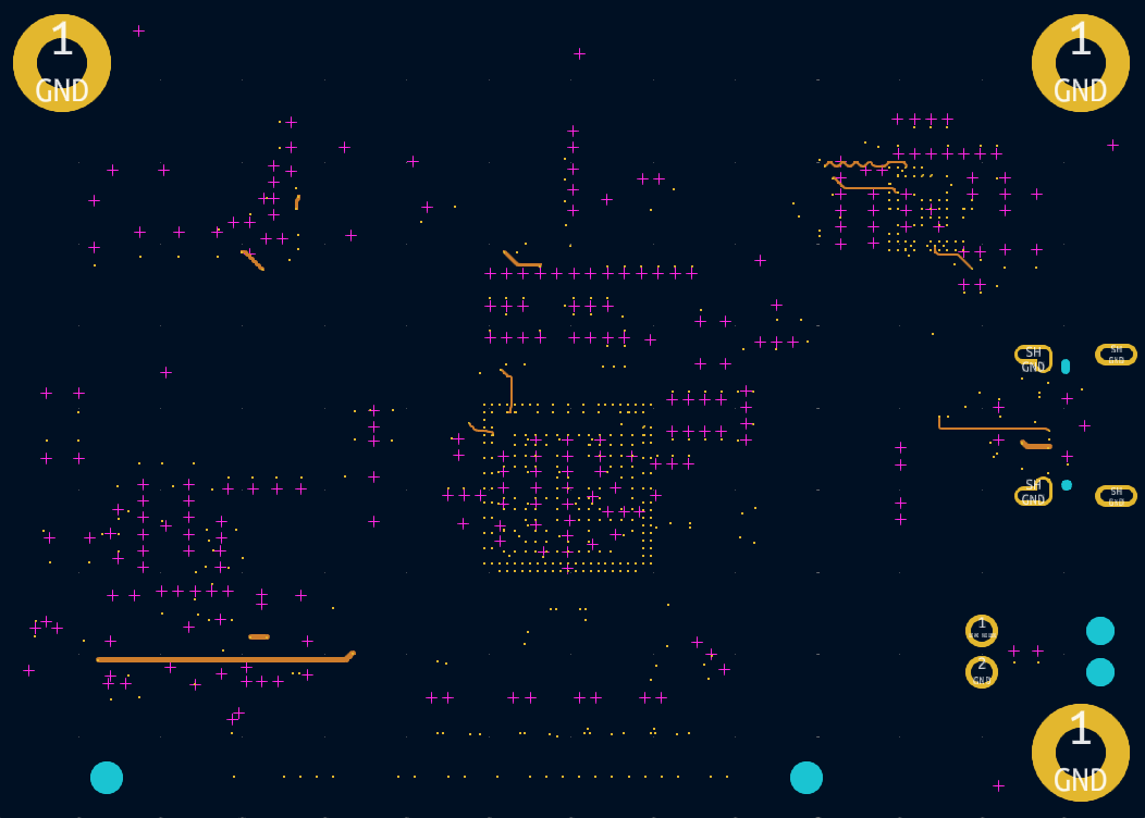
- Automated Board: Components grouped by functional block, with differential pair entry/exit orientations considered during placement to reduce routing crossover. The automated placement was reviewed and a revised placement was used as the basis for the final routed output.
- Impact: Enabled end-to-end routing completion including BGA fanout and differential pair routing, though further placement refinement is expected in future iterations
Key Highlights
Functional Block Grouping
The placement algorithm grouped the Intel JHL6340 controller with its decoupling capacitors, the USB-C connector with its Thunderbolt lane connections, and the PCIe connector with its downstream lane fanout. The DC-DC converter and its associated passives were placed as a separate power block.
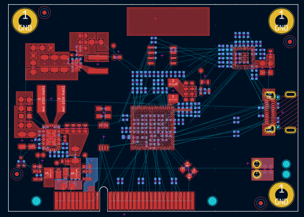
BGA Fanout Routing
The automation produced fully routed fanout from the Intel JHL6340's 337-pad FC-CSP BGA — covering both the 0.65mm-pitch inner grid and the 0.46mm-pitch perimeter rows. This required correct via-in-pad placement and escape routing decisions within tight clearance constraints across all 337 pads, and was completed without manual pad-by-pad configuration.
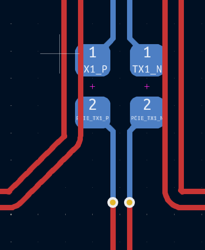
Differential Pair Routing
22 of the 25 differential traces on the board — spanning Thunderbolt 3 upstream pairs and PCIe x4 Gen 3.0 TX/RX lane pairs — were routed by the automation. The remaining 3 pairs require manual completion. Spacing consistency and further refinement remain open improvement areas.
DFA/DFM Report Generation
The automation generated Design for Assembly and Design for Manufacturability reports alongside the routing output, providing engineers with a structured starting point for review rather than requiring manual inspection of every component and clearance.
Automated Routing Process
Following placement, the routing automation handled BGA escape routing, power shape generation for multiple voltage domains, differential pair routing across 22 of the 25 pairs, signal layer assignments, and via placement — producing a substantially routed board file (238/242 signals, 22/25 differential pairs).
🔋 Power and Ground Routing
Power and ground nets are routed with wider traces appropriate to current requirements. Dedicated power layer polygons are generated with smooth, continuous planes rather than fragmented fills, which reduces impedance and simplifies plane review. For dense areas requiring higher current on signal layers, signal pour is used to supplement the distribution.
⚡ Differential Pair Routing
22 of the 25 differential pairs were routed by the automation, covering the Thunderbolt 3 upstream TX/RX pairs and the PCIe Gen 3.0 TX and RX lane pairs to the expansion slot. Where polarity mismatches are present in the schematic, the router applies a crossover to restore correct signal polarity without requiring manual net swaps. The remaining 3 pairs require manual completion.
📏 Bus Length Matching
For interfaces operating above 50 MHz, the router applies bus length matching to keep signals within the timing window required by the interface specification. This is applied during the routing step and covers the parallel buses on this board.
🔌 BGA Pin-Aligned Routing
The Intel JHL6340's 337-pad FC-CSP BGA was routed with pin-aligned escape routing across both pitch zones: the 0.65mm-pitch inner array and the tighter 0.46mm-pitch perimeter rows. The router supports any BGA pitch within the design rules constraints, and all 337 pads were fanned out by the automation without manual pad-by-pad configuration.
🔩 Via Optimization
Via placement is considered during routing to reduce unnecessary layer transitions. The router avoids redundant vias where a signal can continue on the same layer, which reduces via count and simplifies manufacturing review.
📐 Automatic Layer Assignment
When a constraints file is available, the router uses it to determine layer assignments rather than applying a fixed stackup assumption. This allows the routing to reflect the actual stackup and impedance targets defined for the board without manual layer mapping.
Manual Refinement Required
Transparency about automation limitations is important. The automated output for this board is a usable starting point, but requires manual engineering review and refinement before it would be considered production-ready.
🎨 Board Outline Definition
The mechanical board outline must be defined before the automation can begin. The automation works within the provided boundaries; it does not generate board outline geometry.
⚙️ Design Rules Configuration
Design rules — including track widths, differential pair spacing, via sizes, and clearances — are configured through an external rules file that the automation reads at runtime. For a high-speed board like this, these rules require engineering judgment to set appropriately before running automation.
🔧 Placement Refinement
While the automated placement produced a complete and routable arrangement, further refinement of component positioning is an identified improvement area — particularly for the Thunderbolt controller decoupling network, the crystal oscillator, and connector alignment relative to board edges.
✏️ Differential Pair Spacing and Length
Spacing consistency across the 25 differential pairs requires manual verification and correction in areas where the automated router produced inconsistent pair separation. Bus length matching is now applied for signals above 50 MHz; however, fine-grained intra-pair length equalization for PCIe and Thunderbolt lanes may still require manual tuning.
Time Investment Reality
The automated routing completed in approximately 3 hours. Manual refinement time for a board of this complexity — covering differential pair cleanup, placement adjustments, and design rule review — has not yet been formally measured for this board and will be documented in a follow-up update. For reference, a full manual layout of a board at this complexity level would typically require significantly more engineering time.
Automation Strengths
The automation demonstrated several genuine capabilities on this board that would be useful to engineers working through an initial layout study or routing feasibility assessment.
Multi-Hierarchy Schematic Handling
The automation successfully traversed all five sheets of the KiCad hierarchy — top-level, tb, tb-power, power, and connectors — and extracted the functional block structure and net relationships needed to drive placement and routing decisions without manual net list preparation.
BGA Fanout and Pin-Aligned Routing
Escape routing from the Intel JHL6340's 337-pad FC-CSP BGA was handled in full by the automation — covering both the 0.65mm-pitch inner grid and the 0.46mm perimeter rows — with pin-aligned trace exit from the device. Manually setting up fanout for a 337-pad fine-pitch BGA is a time-consuming step that the automation removes from the engineer's workload.
IP Protection
Design automation runs on the local system, keeping design data on the engineer's hardware rather than requiring upload to a cloud service.
Minimal Configuration Setup
Beyond the design rules file and board outline, the automation derived its placement and routing decisions from the schematic directly. Engineers spend less time configuring the tool and more time reviewing and refining the output.
DFA/DFM Report Generation
Alongside the routed board, the automation produced Design for Assembly and Design for Manufacturability reports, giving engineers a structured review document as part of the same run.
Design Results Comparison
Traditional Manual Design
- Significant engineering time for BGA fanout and differential routing at this complexity
- Multiple manual iteration cycles typical for high-speed interface boards
- Requires a layout engineer experienced with BGA escape and differential pair discipline
- Complete engineer control over all placement and routing decisions
- Optimal results achievable with skilled, experienced designer
- Manual verification of all clearances and design rules
Automated Approach
- ~3 hours for automated routing completion
- Manual refinement still required — especially for differential pair spacing and length matching
- Reduces time spent on initial placement and BGA fanout setup
- Schematic-driven, hierarchy-aware design context across all five sheets
- Integrated placement, routing, and DFA/DFM report generation in a single run
- Engineering review and refinement required before production use
Honest Assessment
This automation does not replace the layout engineer, particularly on a board with 25 differential pairs, a 337-pad fine-pitch BGA, and multi-domain power requirements. What it provides is a usable starting point — a substantially routed board (238/242 signals, 22/25 differential pairs) that an engineer can review, adjust, and refine rather than starting from a blank board. It is well suited for initial placement studies, routing feasibility checks, and reducing the time spent on repetitive setup work. Production readiness still requires engineering judgment and manual refinement.
Current Limitations
Transparent assessment of automation limitations is important for setting accurate expectations. The following limitations were identified during this case study.
Differential Pair Length Matching
Bus length matching is applied for interfaces operating above 50 MHz. However, intra-pair and inter-lane fine tuning for PCIe Gen 3.0 and Thunderbolt 3 — particularly meander-based length equalization — may still require manual adjustment to meet the tighter timing margins these interfaces require.
Power Planes for Voltage Regulators
Power polygon generation for voltage regulator outputs requires further refinement. In some configurations the generated planes do not fully capture the intended distribution topology around the regulator, and manual correction is needed before the power delivery network is considered complete.
Placement Improvement Ongoing
The automated placement is a functional starting point but is identified as an area for continued improvement. For a board of this density and interface complexity, further refinement of the placement algorithm is expected to produce better routing channel management and reduce the manual adjustment burden.
Open Issues
The following issues were identified during this case study and remain open for resolution in future development iterations.
⚠️ Fine Tuning
The differential traces required cleanup — 6 pairs were flagged for DFM issues and needed to be corrected before the design could pass review.
⚠️ Placement Quality on Dense High-Speed Boards
The automated placement produced a functional starting point but required fine-tuning. For this case study, the automated placement was reviewed and a revised placement was used as the basis for the final routed output, demonstrating that placement and routing can be run as independent steps when needed.
⚠️ Design Rule Validation Completeness
Basic DRC compliance is achieved, but interface-specific design rules — such as those relevant to PCIe Gen 3.0 or Thunderbolt 3 routing guidelines — require manual verification. Automated checking for protocol-specific constraints is not yet available.
Want to See More Examples?
Review other boards covered in our Case Study section. We document designs using the same automation algorithm across Altium, Cadence, and KiCad platforms.
Request Technical Discussion View More Case Studies