
Quick Navigation
- 1. Why We Need Automation in KiCad?
- 2. How Do We Add Automation to KiCad?
- 3. Target Boards: What We Tested
- 4. What Are the Inputs for the App?
- 5. How Do We Control and Review the Design Generation Process?
- 6. How Do the Placement Results Look?
- 7. How Does the KiCad Autorouting Look?
- 8. What's Great About This Automation?
- 9. What Part of the Design Was Manually Created?
- 10. What Still Needs Work?
- 11. How Do We Compare?
- 12. Frequently Asked Questions
Why We Need Automation in KiCad?
Imagine finishing your schematic, importing it into your PCB editor, and instead of facing a three-day routing marathon, you define your core design rules, click a button, and watch as an intelligent agent places and routes your board in minutes. You're no longer a hard-working engineer doing repetitive tasks; you're a supervisor, free to focus on the high-level, critical aspects of your design. This isn't a fantasy from a million-dollar EDA suite. It's the future we believe is possible with AI PCB automation for KiCad, and it addresses the platform's most significant bottleneck: its entirely manual workflow. Unlike tools such as Altium or Cadence that offer some degree of autorouting, KiCad autorouting has historically depended on external plugins like FreeRouting—and even those require significant manual setup.
In our previous posts, we discussed [how we automate altium ai pcb routing], [why pcb autorouting remains broken] and [why autoplacement requires manual intervention]. While those challenges exist in commercial EDA platforms, KiCad doesn't even have these automation features to begin with. The question we're addressing today: Can we bring effective AI PCB automation to KiCad's manual-only workflow?
How Do We Add Automation to KiCad?
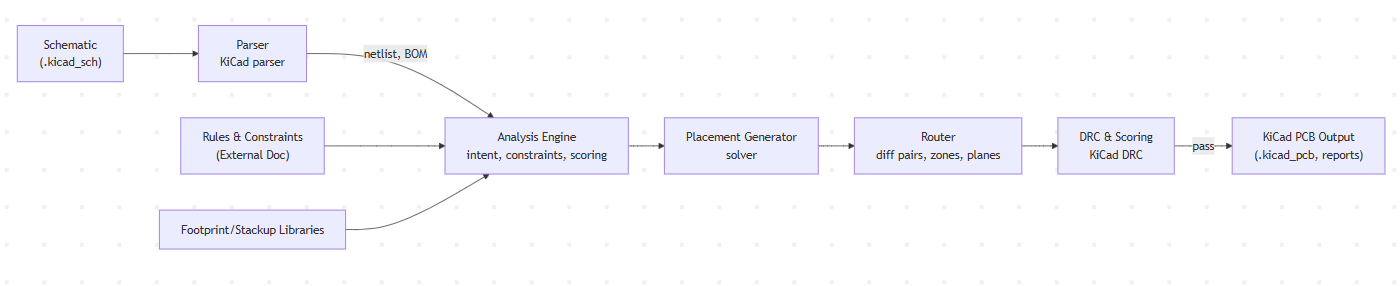
For any effective automatic PCB placement and routing, you need good placement first, then PCB autorouting. Without intelligent component placement, even the best routing algorithms will struggle to produce quality results. To achieve a good understanding of the design, we use the automation pipeline mentioned below and KiCad's Python scripting interface. Our KiCad autorouting process differs from traditional approaches in a fundamental way: we start by reading and understanding the schematic design intent before generating the physical layout.
Our Automation Pipeline
📄 Schematic Analysis
We parse KiCad schematic files (.kicad_sch format) to extract connectivity information, component relationships, and circuit hierarchies. This gives us context that pure netlist-based approaches miss.
🧠 Design Intent Extraction
From the schematic data, we identify functional blocks, power distribution networks, high-speed interfaces, and critical signal paths. This understanding guides our placement and routing decisions.
🔧 KiCad Python Integration
Using KiCad's Python scripting capabilities, we programmatically generate the PCB layout, place components, and create routing paths. Our tool operates as a KiCad AI plugin, working within KiCad's native environment without requiring cloud uploads or external servers.
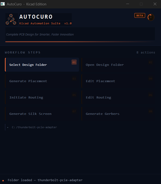
The Tool Interface
The AutoCuro KiCad Automation Suite provides a step-by-step workflow panel that guides engineers through each stage of the design process — from folder selection to Gerber generation.
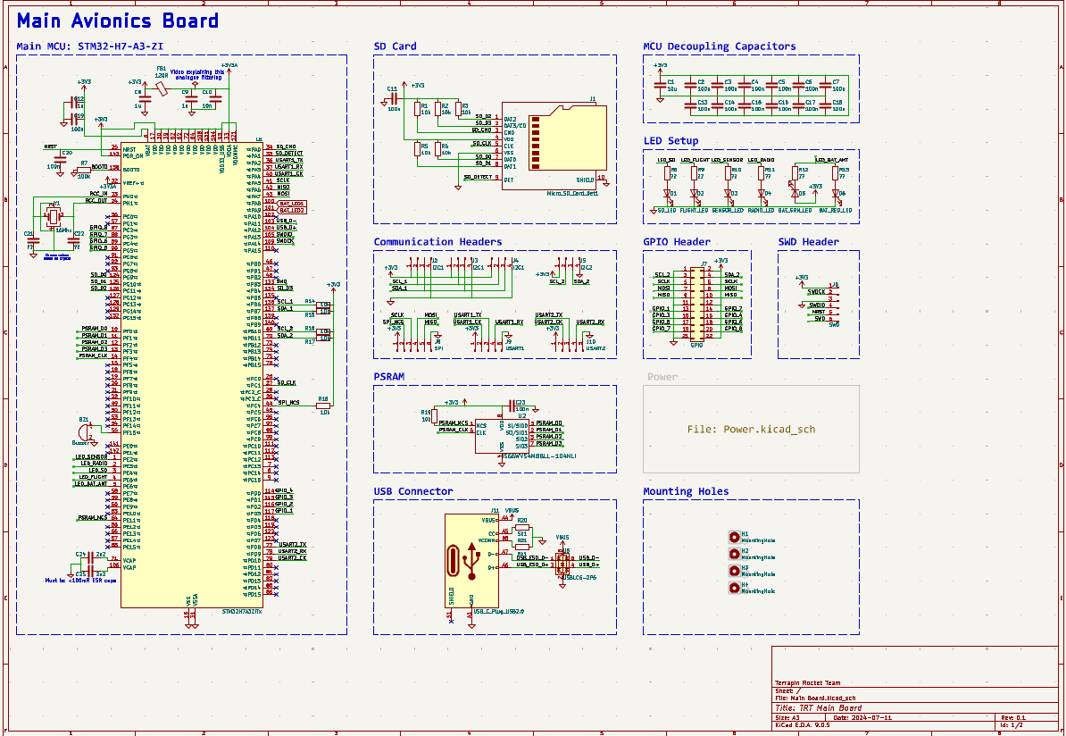
Target Boards: What We Tested
To test and develop our automation approach, we have run it against two real-world open-source designs at different complexity levels. Both boards are documented as separate case studies. In this blog, we discuss the Main Avionics Board from the Terrapin Rocket Team's Student Researched and Developed (SRAD) Avionics project while you can refer to our latest case study [Automated thunderbolt pcie adapter board design in kicad] which overcomes the limitations mentioned in the blog.
Board Specifications
This board includes power management, sensor interfaces, communication peripherals, and the complexity typical of aerospace applications. It's an ideal test case because it represents real engineering requirements rather than a simplified example.
Source: Terrapin Rocket Team GitHub Repository
What Are the Inputs for the App?
Our automation system requires specific inputs from the KiCad design environment:
📋 Required Input Files
- KiCad schematic files (.kicad_sch) - Contains circuit connectivity and hierarchy
- Board file with board outline and component footprints kept outside the board outline
- Design rules - Track widths, clearances and layer stackup. These are added through external document
How Do We Control and Review the Design Generation Process?
Using our app we allow the code to be run through various stages so that the user has control over every stage and does not waste time while running a large design cycle. Following stage outputs are available which can be iterated again and again: Placement, Routing and Gerber generation. Engineers need visibility into what the automation is doing and the ability to guide the process.
Reviews Done During Every Process
🔍 1. Check for Netlist Errors
Verification of netlist integrity and connectivity before processing begins.
📚 2. Library Mismatch
Detection of component footprint and library inconsistencies.
📊 3. Placement Scores
Generated based on the dynamic rules created for the database.
🏭 4. DFA/DFM Checks
Design for Assembly and Design for Manufacturing validation.
✅ 5. Routing Scores
Evaluation of routing quality and completion metrics.
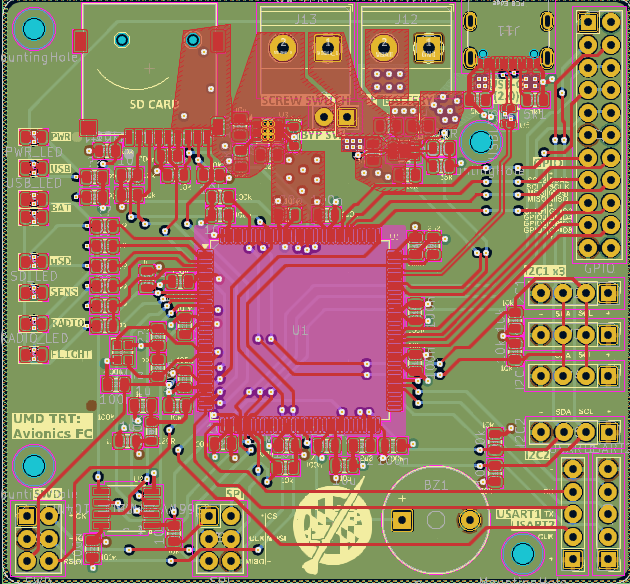
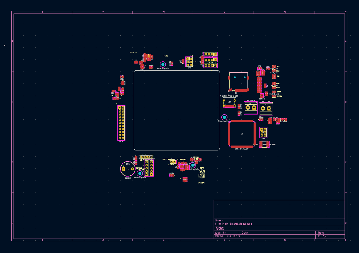
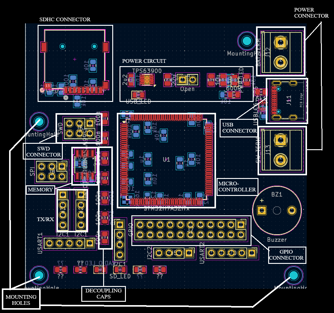
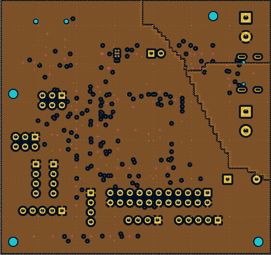
How Do the Placement Results Look?
Placement quality directly impacts routing success. Our approach focuses on understanding circuit functionality to create logical component groupings.
Placement Features
🎯 Circuit-Aware Grouping
Components are grouped based on their functional relationships identified from the schematic. Power management circuits stay together, sensor interfaces are clustered, and the MCU support circuitry is properly organized around the processor.
⚡ Critical Component Positioning
Decoupling capacitors are automatically placed close to their associated power pins. Crystal oscillators and their load capacitors maintain proper geometric relationships.
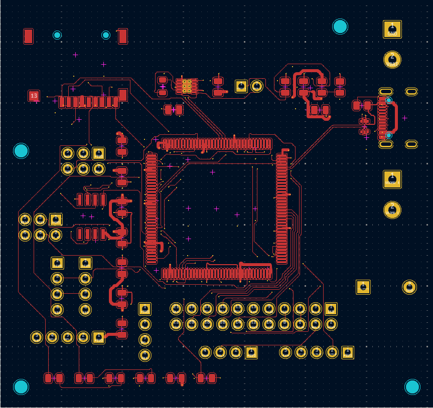
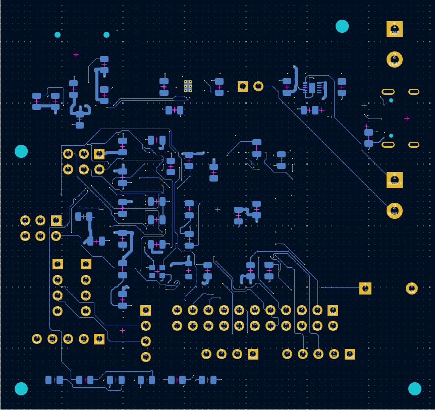
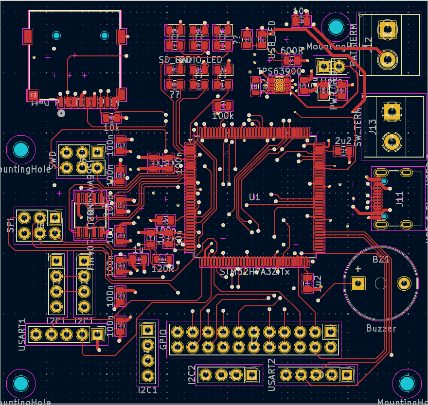
How Does the KiCad Autorouting Look?
After placement, our KiCad autorouting algorithms do the following: Power plane decision, power supply fanouts, stackup selection if not input, differential nets routing strategy, via optimization, routing of traces, cleanup. If you've used the KiCad FreeRouting plugin before, the overall stage sequence will feel familiar—but the schematic-driven decisions are what differentiate this approach.
Routing Completion
The AI PCB automation completed routing across signal layers and power planes. However, like all PCB autorouting approaches, not everything was perfect on the first pass.
What's Great About This Automation?
✅ Genuine Advantages
What Does the Tool Automate?
The tool automates component placement and PCB routing, running entirely from your desktop. Starting from your KiCad schematic and input design constraints, it handles: component placement across the board (balancing mounting hole positions, edge components, functional block grouping, power distribution, and differential routing constraints), followed by power plane generation and complete trace routing. The tool also generates DFA and DFM reports as part of the output. Tasks that would typically take a layout engineer half a day to a full day for placement alone are handled in approximately 5 minutes, depending on the system.
Schematic-Driven Intelligence
By starting with schematic analysis, the AI PCB automation understands circuit intent. This produces more logical placement and routing decisions compared to purely netlist-based approaches.
IP Protection
We generated this design using automation algorithms which run from your system, keeping your design data secure on your own hardware.
Minimal Configuration Setup
Unlike traditional PCB autorouting tools that require extensive constraint definition, our approach extracts most requirements directly from the schematic. Engineers spend less time configuring the tool and more time reviewing results.
Integrated Workflow
The AI PCB automation process handles both placement and routing in a coordinated manner, considering how placement choices affect routing outcomes. This integration improves overall results. The algorithm is known to work reliably on latest KiCad versions ver8 and ver9.
What Part of the Design Was Manually Created?
Transparency is important. Our automation doesn't eliminate the need for engineering judgment—it reduces repetitive work.
Manual Design Elements
🎨 Board Outline Definition
The mechanical board shape, mounting holes, and connector locations were defined manually based on the enclosure requirements. Automation needs these boundaries to work within. Board footprints are expected by default.
📍 Predefined Constraint
You can suggest connector or component positions beforehand by defining the rough location where you want certain components. This allows the automation to work within your preferred layout structure while optimizing the surrounding placement.
⚙️ Design Rules Setup
Design rules are set up using an external document which the app reads while running. This allows for easy configuration of track widths, clearances, and via sizes specific to your project requirements.
🔧 Final Placement Refinement
The automated placement was modified for crystal and decoupling capacitors, as well as power blocks to make them more routable. These adjustments ensured optimal signal paths and power distribution.
✏️ Final Routing Refinement
After automated routing, the design required manual review and cleanup. Differential traces, even though routed, needed refinement. Power planes on the top layer had to be redrawn. Some signals had to be rerouted for optimal signal integrity and electrical performance.
Time Investment Reality
The automated portion (placement + routing) took approximately 10 minutes. Manual refinement and optimization required an additional 3 hours of engineering time. This is still significantly faster than full manual design, which could take 16-24 hours for a board of this complexity.
What Still Needs Work?
We're committed to honest assessment of our technology. Here are the areas where improvement is needed:
⚠️ Current Limitations
Via Optimization
The automated routing sometimes generates more vias than necessary. While functionally correct, reducing via count would improve signal integrity and reduce manufacturing costs. Manual via consolidation was required.
Trace Length Matching
For high-speed differential pairs and parallel buses that require length matching, the automation currently lacks sophisticated tuning capabilities. These traces required manual adjustment to meet timing requirements.
Board Complexity
If the size of the board reduces wherein the placement has to be done, it is possible that the current algorithm would struggle. We would be adding another board study which would show more components on a board having higher component and routing complexity.
Scalability Testing Ongoing
This avionics board represents moderate complexity. We're continuing to test the automation with larger designs to understand scalability limits and identify optimization opportunities.
How Do We Compare?
An honest comparison of PCB autorouting vs manual routing requires acknowledging that different approaches have different strengths. Here's how KiCad autorouting options stack up:
KiCad Manual Routing
- Complete engineer control over all decisions
- Optimal results for experienced designers
- Time-intensive: 16-24 hours for this board complexity
- Requires deep understanding of design intent
- No automated assistance for repetitive tasks
KiCad FreeRouter Plugin
- Rule-based PCB autorouting without schematic awareness
- Effective for simple or highly constrained routing tasks
- Requires significant setup and tuning of design rules
- Limited understanding of placement and signal intent
- Often produces suboptimal results requiring heavy cleanup
KiCad AI PCB Automation
- Schematic-driven AI PCB automation provides design context
- Integrated placement and PCB autorouting optimization
- ~10min automation + 3 hours refinement
- Works within KiCad's native environment
- Still requires manual optimization for production
The Honest Assessment
Our AI PCB automation doesn't replace skilled PCB designers. Instead, it handles the repetitive aspects of layout work, allowing engineers and managers to increase productivity and reduce layout time and shorten time to market.
Frequently Asked Questions
Want to See More Examples?
Check other boards covered in Case Study section. We cover boards designed using same AI PCB automation and PCB autorouting algorithm in Altium, Cadence, KiCad and other tool series.
Request Technical Discussion View More Case Studies