
Quick Navigation
Context: Why We Built This
In our previous posts, we analyzed why traditional autorouting is broken and autoplacement requires manual intervention. Today, we're sharing our honest assessment of what we've built to address these challenges.
The reality is that existing autorouting and autoplacement tools have fundamental limitations that prevent them from delivering production-ready results. Rather than just critiquing existing solutions, we decided to build our own automation technology specifically designed for embedded hardware applications. But the question remains: Is it actually any good?
The automation algorithm is designed to behave like an Altium AI Assistant, assisting engineers with placement and routing decisions rather than replacing manual design control.
We have divided this article into sections covering Altium automation flow, inputs required, placement results, and routing results.
Validation Boards
Before describing the automation flow, here are the real boards used to validate the tool:
- STM32L496G-DISCO — placement and routing tested
- STM32MP257F-EV1 — placement and routing tested
These boards were chosen because they expose common embedded PCB challenges: dense component placement, BGA breakout, power routing, differential pairs, and connectors — all of which require manual review after automation. We have several PCB design databases where this algorithm has been run.
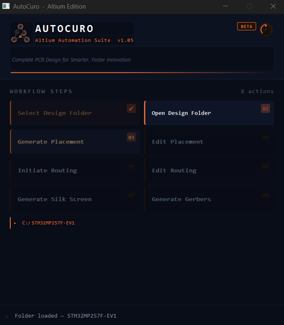
Altium Automation Flow
Here's how our Altium automation process works from start to finish:
Schematic Import
Import your Altium schematic files. Our tool reads the design hierarchy, component data, and connectivity information.
Constraint Extraction
Design rules are read from your schematic and external configuration. Track widths, clearances, and layer stackup are parsed automatically.
Placement Generation
Components are placed based on circuit topology and design constraints. The algorithm considers functional grouping and routing feasibility.
Routing Execution
Automated routing connects all nets while respecting design rules. Power distribution and signal routing are handled in coordinated passes.
Export to Altium
The completed design is exported back to Altium format for review, refinement, and manufacturing output generation.
What Are the Inputs?
Our automation system requires specific inputs from the Altium design environment:
📋 Required Input Files
- Altium schematic files (.SchDoc) - Contains circuit connectivity and hierarchy
- Board file with board outline defined
- Component footprints placed outside the board outline
⚙️ Design Rules Configuration
- Track widths and clearances
- Via sizes and drill specifications
- Layer stackup configuration
- These are added through an external configuration document
🎯 Optional Inputs
- Predefined component positions - specify rough locations for connectors or critical components
- Keep-out zones and mechanical constraints
How Do We Control the Process?
Our app runs through discrete stages, giving you control at each step without wasting time on full design cycles. You can iterate on placement, routing, and output generation independently.
Reviews at Each Stage
🔍 1. Netlist Verification
Verification of netlist integrity and connectivity before processing begins.
📚 2. Library Mismatch Detection
Detection of component footprint and library inconsistencies.
📊 3. Placement Scoring
Placement quality metrics generated based on design rules.
🏭 4. DFA/DFM Checks
Design for Assembly and Design for Manufacturing validation.
✅ 5. Routing Completion Metrics
Evaluation of routing quality, completion percentage, and rule violations.
Component Placement: What We've Achieved
Features
🎯 Target Applications
Our algorithms are best fit for IoT, industrial, and general embedded hardware.
📊 Capacity and Board Fill
- We can achieve good placement up to 75% board fill. By board fill, we mean the ratio of component-outline area to board-outline area.
- Currently able to handle 1000+ component boards without breaking constraints
🧠 Intelligent Circuit Recognition
Our system understands circuit designs. We use your data and constraints to generate the PCB placement design.
🔧 Tool Compatibility
The algorithm works with Altium, Cadence, and KiCad platforms.
Limitations
Scalability and Testing
For larger designs, our tests are still ongoing.
Complex Board Limitations
Higher packing ratios where we cannot do super complex boards yet.
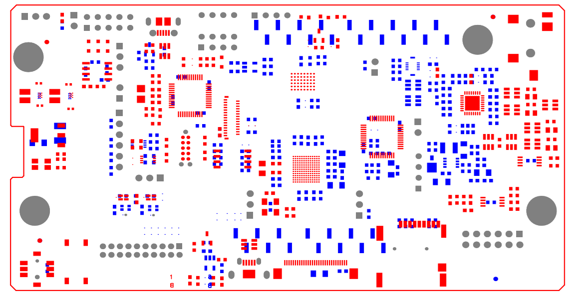
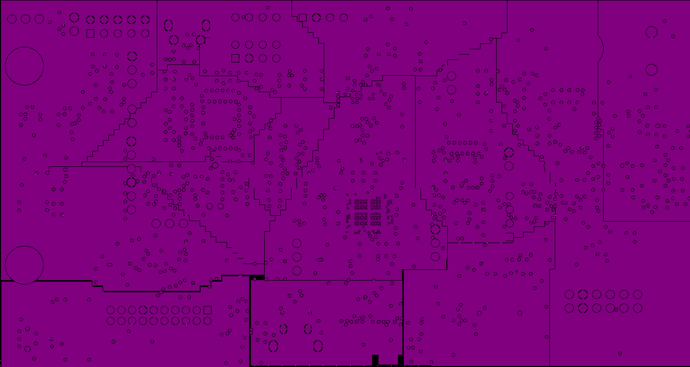
Placement Results
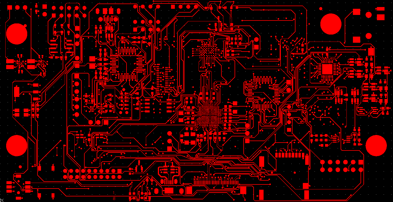
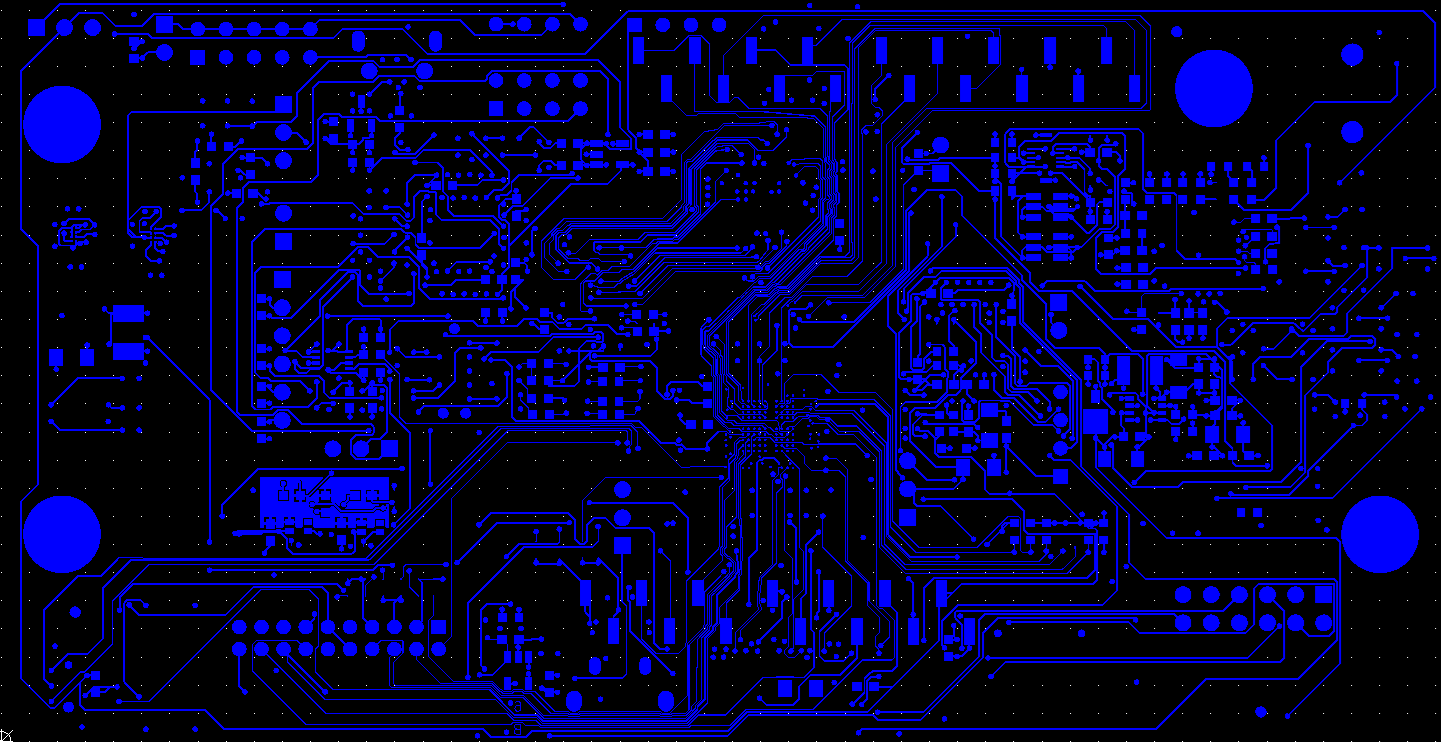
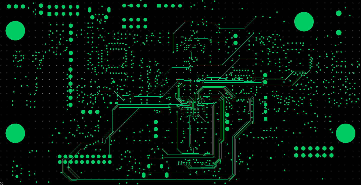
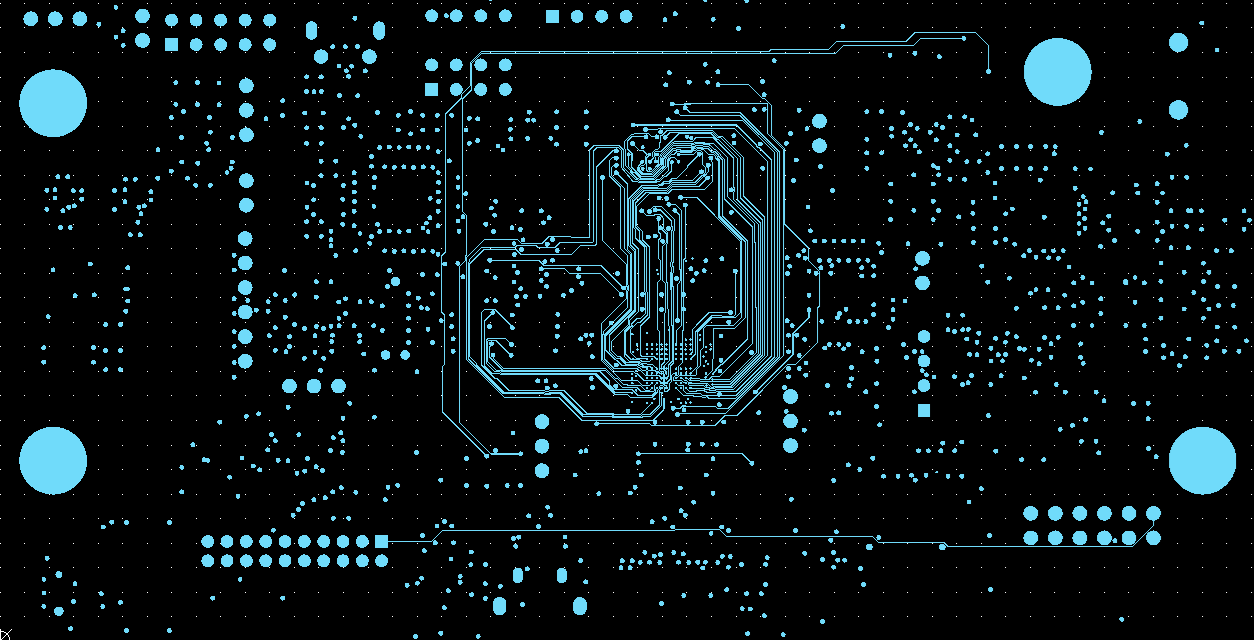
Our Routing Results
These images show routing output from one of our smaller validation boards. The engineer did not have to set up the project manually. Routing took 30-120 minutes, depending on board size. The engineer then spent about 6 hours refining the routing and improving the traces for that board.
For more details visit our GitHub repository.
Results: The Good and The Bad
✅ What Works Well
Speed and Completion Rate
We use our own autorouting algorithms to complete routing within 30-120 minutes for smaller validation boards, depending on board size. On this class of board, we achieve about 80% routing completion before engineer review and refinement.
Automated Gerber Generation
Automatic Gerber generation once the design is approved for release.
DFA and DFM Integration
DFA checks are automated and reports get generated automatically, ensuring manufacturing compatibility.
Design Data Security
The tool runs locally on the engineer's machine. Design files — schematics and layout — are never uploaded to any cloud server. Your IP stays on your hardware.
What Still Needs Work
Manual Intervention Required
Manual intervention is still required for incomplete traces, extra via removal, and trace cleanup. For the smaller validation board shown above, manual refinement took about 6 hours.
Power Plane Optimization
Power planes need some more tweaking to achieve optimal performance.
Case Studies
We document our automation results on real boards, including where the tool falls short. Both case studies below use publicly available ST evaluation boards so the design constraints and complexity can be independently verified.
STM32L496G-DISCO — Placement Case Study
A 6-layer, 336-component board with a 169-pin BGA processor. This case study covers automated component placement only: functional grouping, decoupling capacitor placement, connector positioning, and Altium export. Placement completed in under 30 minutes with all components within board outline and no rule violations.
STM32MP257F-EV1 — Placement and Routing Case Study
A 6-layer evaluation board with a TFBGA436 processor, DDR4 memory, triple Gigabit Ethernet, and multiple mixed-signal interfaces — a significantly more complex board than the L496G. This case study covers both automated placement (~10 minutes) and routing (~5 hours), along with an explicit breakdown of what still required engineering involvement: differential pair length matching, via count reduction, power plane splits, and manufacturer-specific DRC verification.
Want to See More Examples?
If you'd like to see our tool flow with more examples or have specific questions about our automation approach, we'd be happy to share more details.
Request Technical Demo View More Examples