Project Overview
This case study documents the automated design of an STM32 avionics board using KiCad PCB automation. Rather than marketing claims, we present an honest assessment of what current automation technology can achieve, including the manual refinement still required for production-ready results.
| Specification | Details |
|---|---|
| Design Tool | KiCad (Latest Version Compatible) |
| Microcontroller | STM32 Series |
| Application | Avionics System Control |
| Board Layers | 4-Layer Design |
| Routing Complexity | Easy-Medium |
| Key Signals | USB, Differential Pairs, Power Distribution |
Design Challenge
Avionics boards present specific design requirements that test automation capabilities. This project required handling multiple design constraints simultaneously while maintaining signal integrity and power distribution quality.
📍 Component Placement Constraints
Board outline is required for automated placement to work.
🎯 Design Intent Understanding
Automation needed to understand circuit functionality from schematic analysis to make intelligent placement decisions for related components.
🔌 Power Distribution Complexity
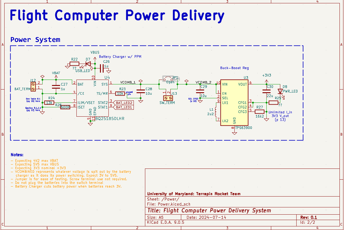
Multiple voltage domains requiring careful power plane design and decoupling capacitor placement for stable operation of the STM32 microcontroller and peripheral circuits.
Automation Approach
The automation process integrated both placement and routing optimization, working from schematic analysis through to manufacturable design files.
Schematic-Driven Intelligence
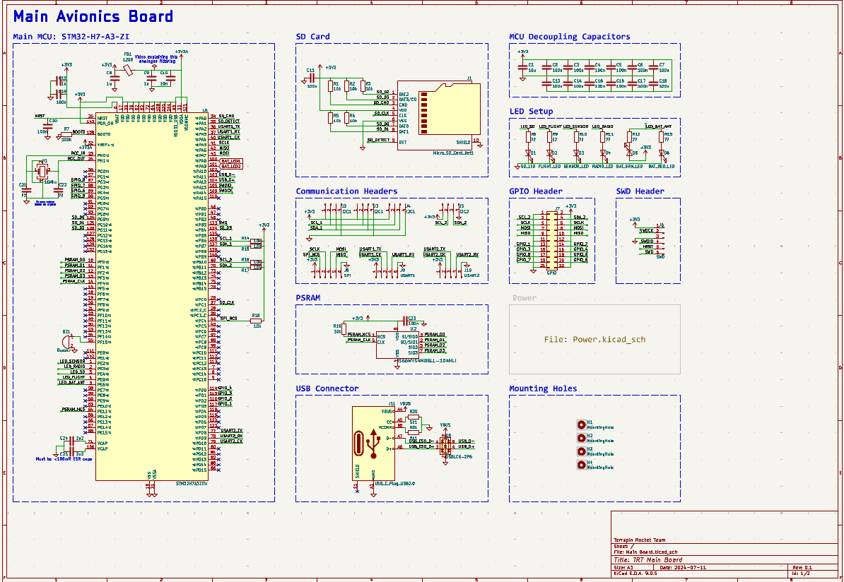
The automation extracted design intent directly from the schematic, identifying circuit blocks and their relationships. This schematic-driven approach allowed the placement algorithm to understand functional groupings without extensive manual configuration.
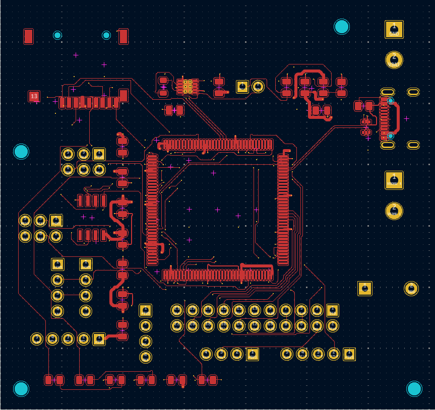
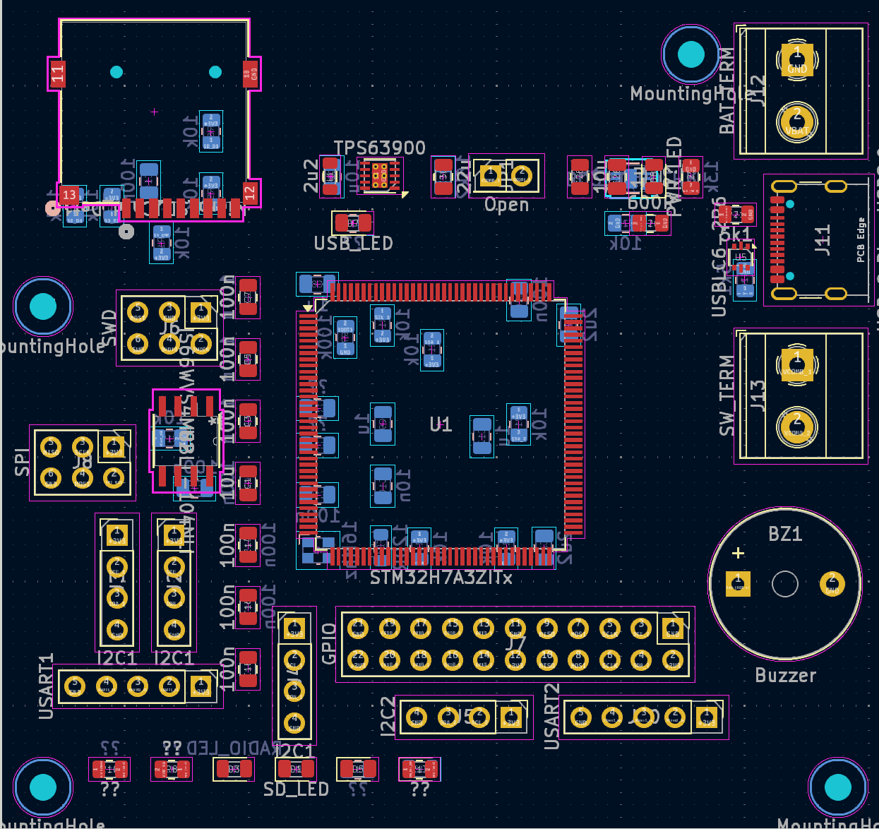
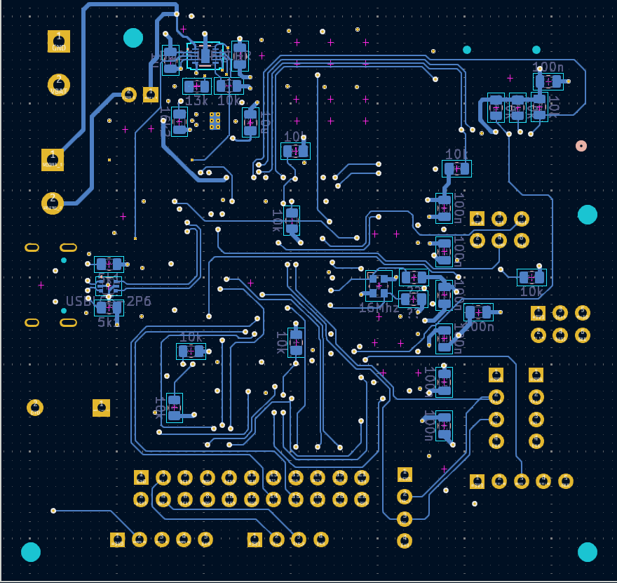
Automated Component Placement
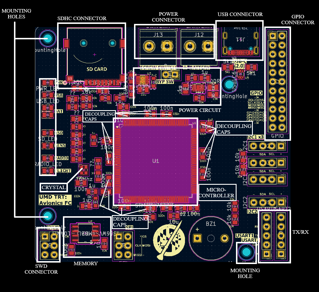
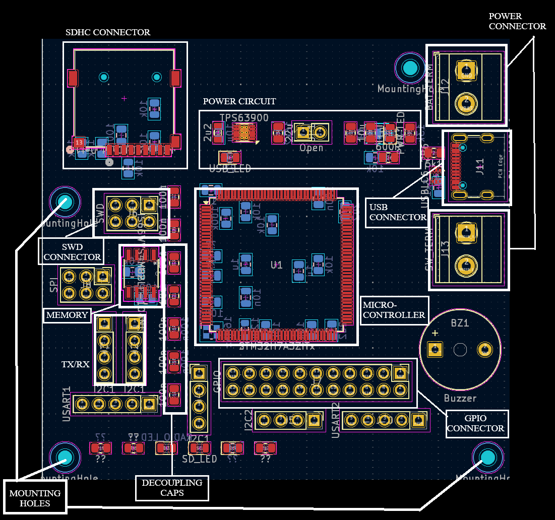
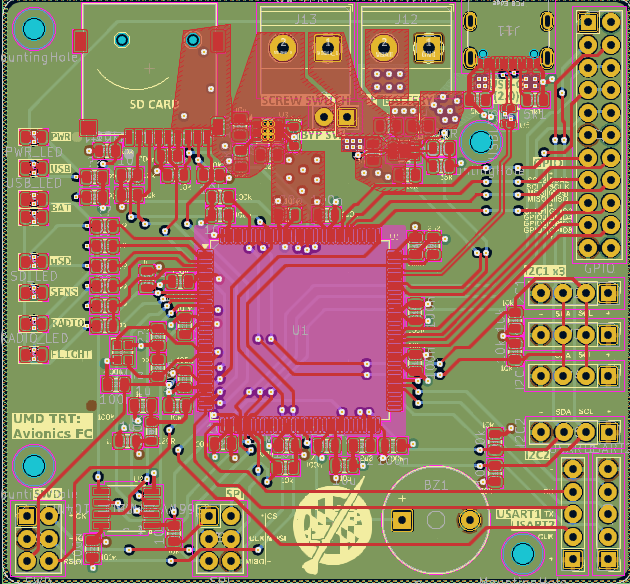
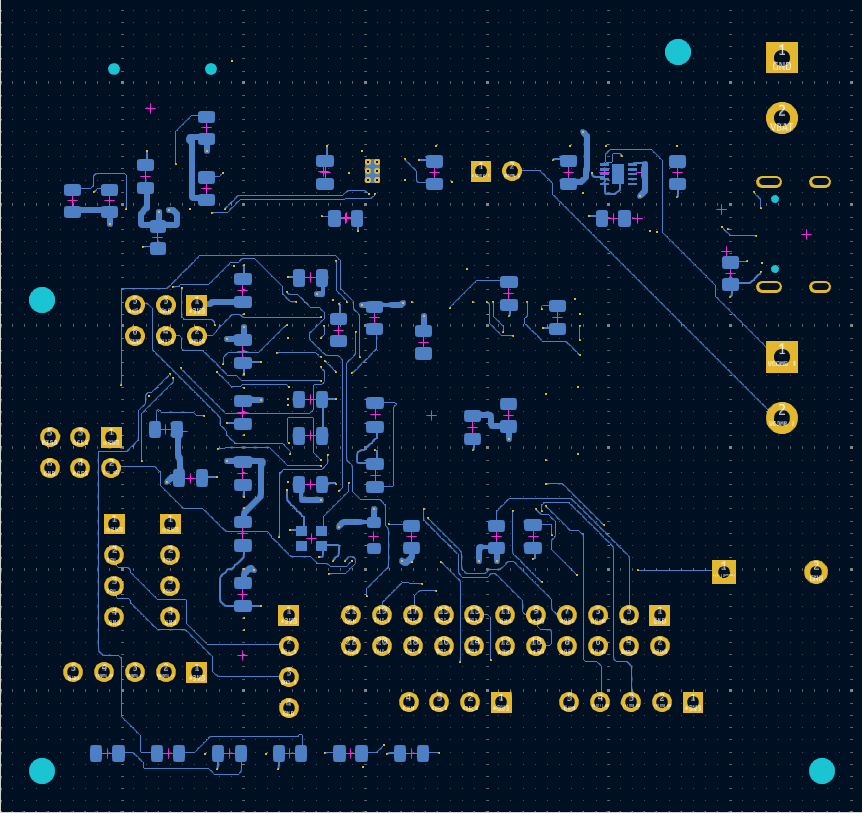
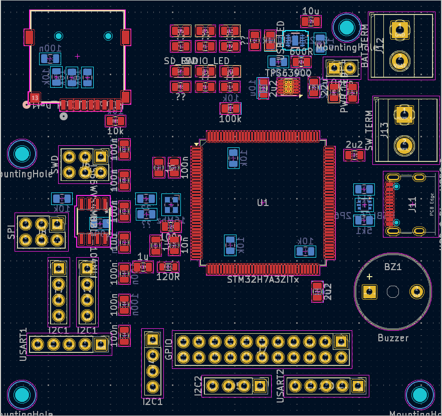
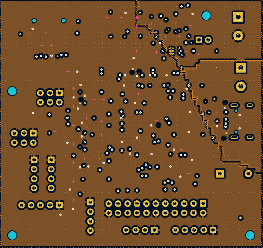
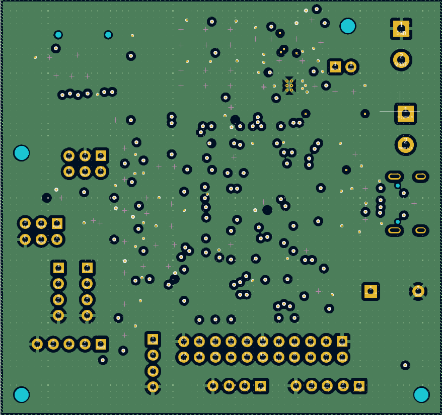
One notable distinction between the original STM32 avionics board and the automated design lies in component placement distribution. The original manually designed board utilized only the top layer for all component placement, whereas the automated design leveraged both the top and bottom sides to improve routing efficiency and overall board compactness.
Placement Strategy Difference
The automated layout system intelligently utilized both sides of the PCB to minimize routing congestion and reduce total trace length. This dual-side placement allowed improved space utilization and signal separation, particularly beneficial for high-speed and power-sensitive circuits.
- Original Board: All components placed on top side only
- Automated Board: Components distributed across both top and bottom sides
- Impact: Better routing balance, reduced via count, and improved signal flow efficiency
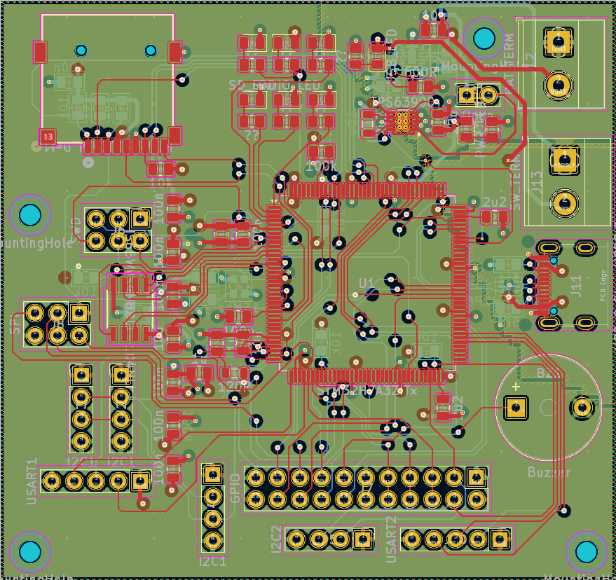
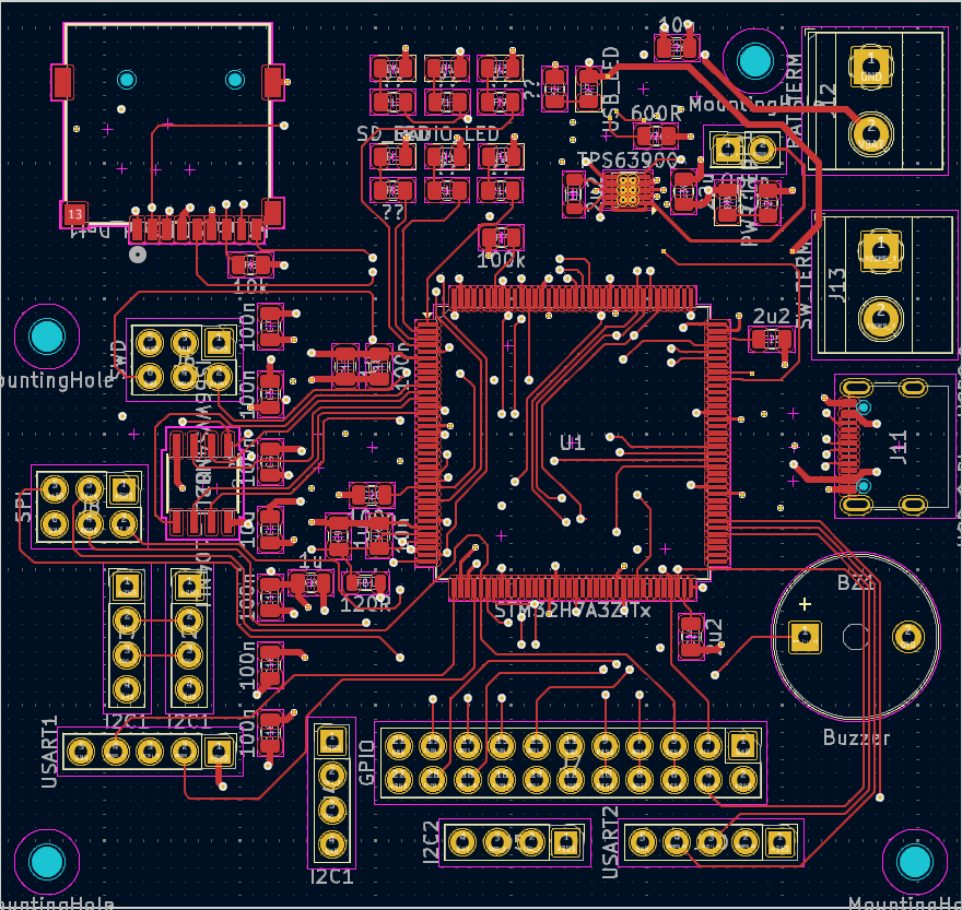
Ratnet Comparison
Before routing, the ratnet view illustrates how component placement impacts the total connection complexity and net overlap. Comparing the original board and the automated board highlights the impact of dual-side placement and optimized grouping on routing efficiency.
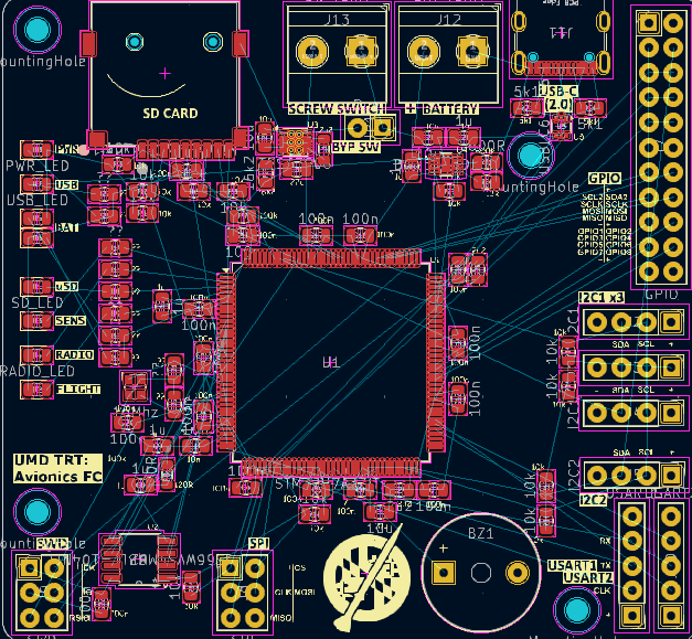
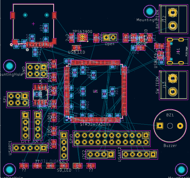
Ratnet Complexity and Optimization
The automated design achieved a significant reduction in visual net congestion and crossover density. This improvement is a direct result of functional grouping and multi-layer component distribution.
- Original Ratnet: High density of overlapping net connections due to all-top-side component placement.
- Automated Ratnet: Dual-side placement reduced net intersection density and improved routing clarity.
- Result: Cleaner ratnet structure leading to more efficient automated routing and fewer vias.
Key Highlights
Intelligent Functional Grouping
The placement algorithm automatically grouped related components including the STM32 microcontroller with its decoupling capacitors, crystal oscillator circuits, power regulation blocks, and connector interfaces. This grouping considered both electrical connectivity and signal flow requirements.
Multi-Objective Decision Making
Placement decisions balanced mounting hole clearances, edge component positioning, routing channel availability, power plane distribution, differential routing requirements, and electrical constraint compliance simultaneously.
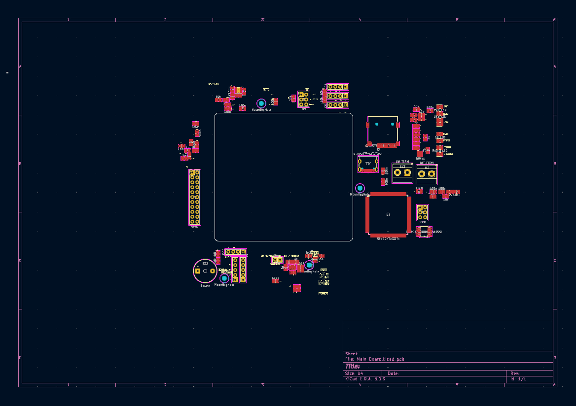
Board Dimension Compliance
All components placed within the defined board outline while maintaining manufacturability clearances and component accessibility for assembly and testing.
Bottom Side utilization
The automated layout system intelligently utilized both sides of the PCB to minimize routing congestion and reduce total trace length. This dual-side placement allowed improved space utilization and signal separation, particularly beneficial for high-speed and power-sensitive circuits.
Automated Routing Process
Following placement, the routing automation handled power plane generation, signal routing, differential pair management, and via optimization in a coordinated workflow.
🔋 Power Plane Generation
Automated creation of power and ground planes with proper via stitching and thermal relief patterns. Power supply fanouts generated from voltage regulators to distribution points.
⚡ Differential Routing Strategy
USB differential pairs routed with controlled spacing and length. Routing algorithm attempted to maintain pair coherence and minimize stub lengths.
🔌 Signal Layer Optimization
Traces routed across signal layers with automatic layer transitions and via placement. Routing considered track width requirements and clearance rules.
Manual Refinement Required
Transparency about automation limitations is important. The automated output required manual engineering refinement before production readiness.
🎨 Board Outline Definition
The mechanical board shape was defined manually based on enclosure requirements. Automation works within these predefined boundaries.
⚙️ Design Rules Configuration
Design rules configured through external documentation that the automation reads during execution. This includes track widths, clearances, and via sizes specific to the manufacturer requirements.
🔧 Placement Refinement
Crystal oscillator positioning and decoupling capacitor placement were adjusted manually to improve routability. Power regulation components repositioned for optimal thermal and electrical performance. USB placement was manually adjusted.
✏️ Routing Refinement
Differential traces required manual adjustment for consistent spacing and impedance control. The traces were rerouted with more spacing and cleanup was done.
Time Investment Reality
Automated portion including placement and routing completed in approximately 10 minutes. Manual refinement and optimization required an additional 3 hours of engineering time. This represents significant time savings compared to 16-24 hours for complete manual design of this complexity level.
Before/After Manual Refinement
The manual refinement phase for this board was completed in partnership with Semicongate. Their engineering team applied company-specific layout practices, design policies, and manufacturing guidelines to elevate the automated output to production-ready quality. This collaboration ensured that sensitive components such as crystals, regulators, and few important interfaces were updated.
Final Production Ready Board
Following the automated placement and routing process and the subsequent manual refinement performed by Semicongate, the design was finalized into a fully production-ready PCB layout.
The final board reflects both the speed of automation and the precision of professional engineering refinement, combining efficient routing, improved signal integrity, controlled impedance paths, and robust power delivery.
Automation Strengths
The automation demonstrated several genuine capabilities that improved design productivity.
Intelligent Agent Performance
The placement task that would require half a day to a full day for a layout engineer was completed in 5 minutes. The agent balanced multiple competing objectives including mounting hole placement, edge components, routing channels, power plane distribution, differential routing, and electrical constraints. This tool is very useful for initial placement assessment and also checking the routing flow.
Schematic-Driven Intelligence
Starting with schematic analysis allowed the automation to understand circuit intent, producing more logical placement and routing decisions compared to netlist-only approaches.
IP Protection
Design automation runs from the local system, keeping design data secure on user hardware rather than requiring cloud uploads.
Minimal Configuration Setup
Unlike traditional autorouting tools requiring extensive constraint definition, this approach extracts most requirements directly from the schematic. Engineers spend less time configuring tools and more time reviewing results.
Integrated Workflow
The automation handles both placement and routing in a coordinated manner, considering how placement choices affect routing outcomes. The algorithm works reliably on latest KiCad versions.
Design Results Comparison
Traditional Manual Design
- 16-24 hours of design time
- Multiple design iterations
- Requires experienced layout engineer
- Complete control over all decisions
- Optimal results for skilled designers
- Manual verification of all constraints
Automated Approach
- 10 minutes automation time
- 3 hours manual refinement
- Reduces repetitive placement work
- Schematic-driven design context
- Integrated placement and routing
- Still requires engineering review
Honest Assessment
This automation does not replace skilled PCB designers. It handles repetitive aspects of layout work, allowing engineers to focus on critical design decisions and optimization. The technology reduces time to market while requiring engineering judgment for production-ready results. This tool is perfect for someone wanting quick placement study and pre-routing
Current Limitations
Transparent assessment of automation limitations helps set realistic expectations for technology capabilities.
Via Optimization
Automated routing generates more vias than necessary in some areas. While functionally correct, reducing via count improves signal integrity and reduces manufacturing costs. Manual via consolidation was required.
Trace Length Matching
High-speed differential pairs and parallel buses requiring length matching lack sophisticated tuning capabilities in current automation. These traces required manual adjustment to meet timing requirements.
Scalability Testing Ongoing
This avionics board represents moderate complexity. Continuing tests with larger designs will identify optimization opportunities and scalability boundaries.
Open Issues
The following issues remain open for resolution in future development iterations:
⚠️ Via Count Optimization
Algorithm generates functionally correct but non-optimal via counts. Requires additional optimization logic to minimize via usage while maintaining connectivity and signal quality.
⚠️ Length Matching Automation
No automated length matching capability for high-speed buses and differential pairs. Manual tuning required for timing-critical signals. This limitation affects memory interfaces and high-speed communication protocols.
⚠️ Differential Pair Consistency
While differential pairs are routed, spacing consistency and impedance control require manual verification and adjustment. Automated impedance calculation needs refinement.
⚠️ Crystal and Sensitive Circuit Placement
Crystal oscillators and sensitive analog circuits require manual placement refinement. Automated placement does not fully account for noise sensitivity and optimal grounding strategies.
⚠️ Design Rule Validation Completeness
While basic DRC compliance is achieved, some manufacturer-specific rules require manual verification. Automated design rule checking needs expansion for comprehensive manufacturing readiness.
Want to See More Examples?
Review other boards covered in our Case Study section. We document designs using the same automation algorithm across Altium, Cadence, and KiCad platforms.
Request Technical Discussion View More Case Studies