
Quick Navigation
Why We Tested LLMs for PCB Verification
PCB design verification is exhausting. A comprehensive design review for a complex board involves checking 200+ individual parameters across 11 major verification phases. As hardware engineers, we wondered: could large language models like ChatGPT and Gemini help automate even a fraction of this work?
The promise seemed reasonable. LLMs can analyze code, understand technical documentation, and reason about complex systems. PCB design data is structured and follows clear rules. Why couldn't an LLM review a pcb design, check component placement, or flag routing violations?
So we decided to test this hypothesis with real hardware: two STM32-based boards with varying complexity levels. We are keen to use LLMs in our PCB automation workflows. These experiments with ChatGPT and Gemini were our first step: can they actually verify a design?
Test Setup: Real Boards, Real Data
Test Subjects
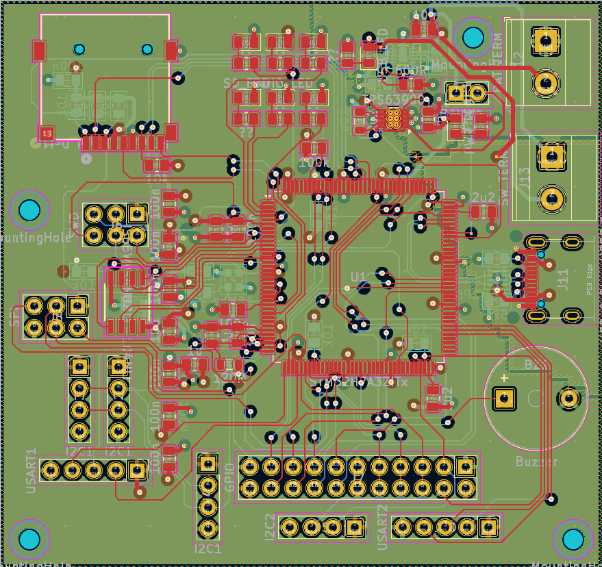
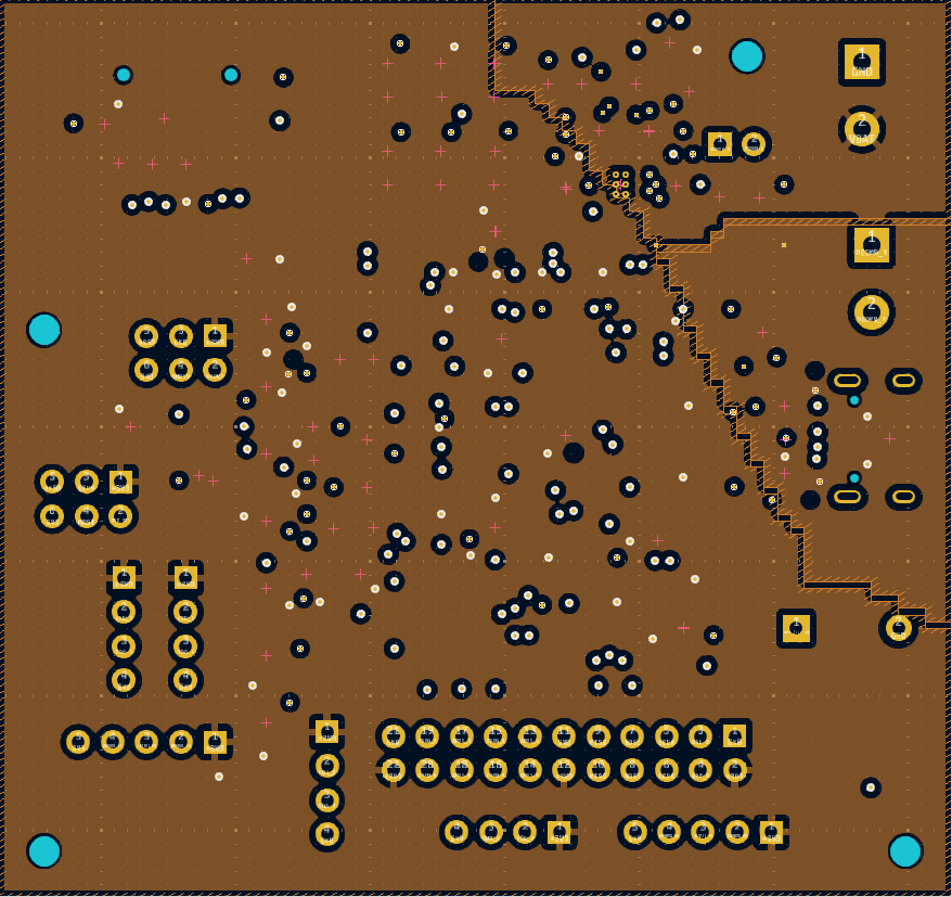
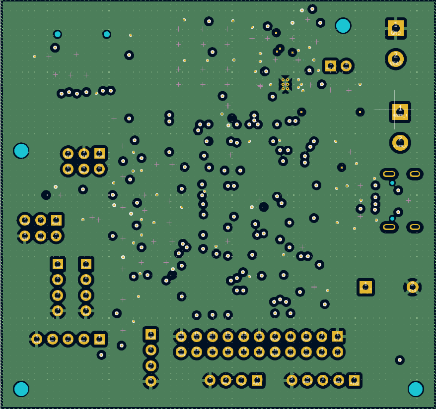
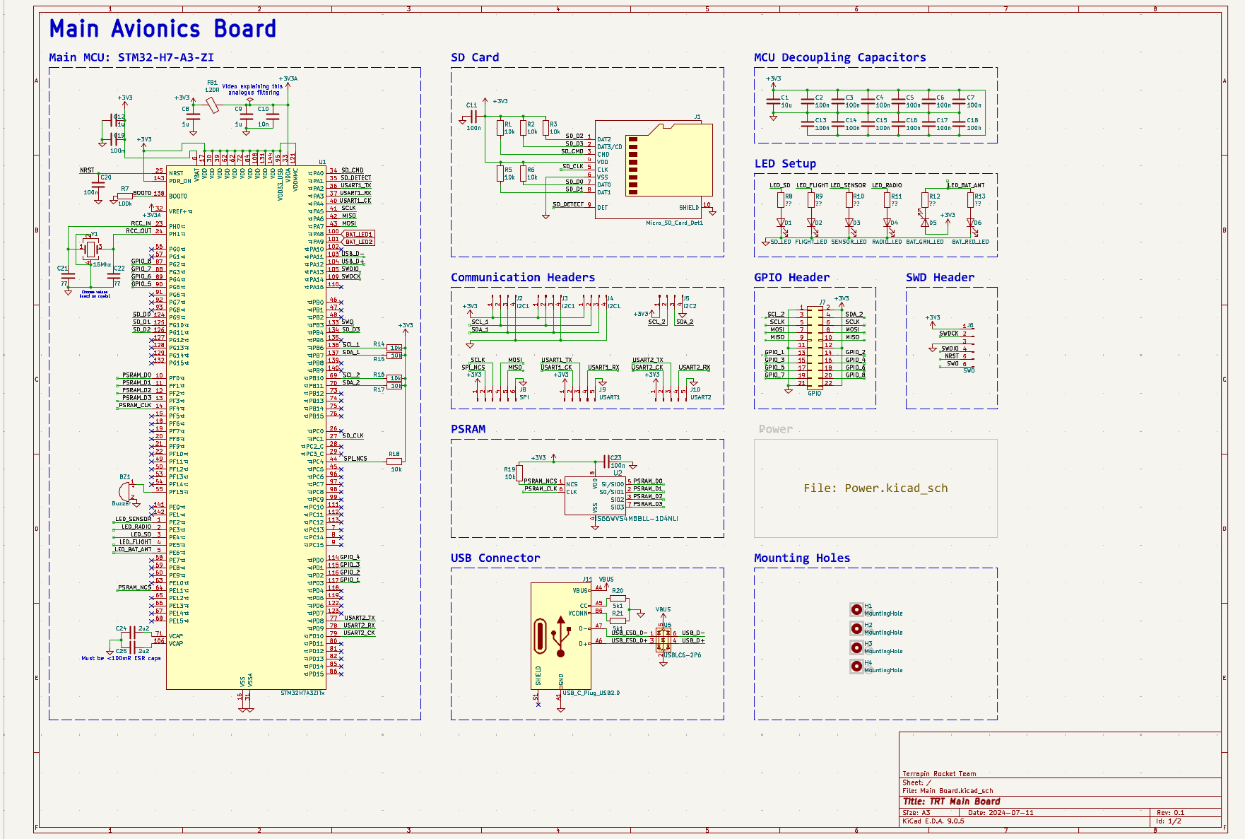
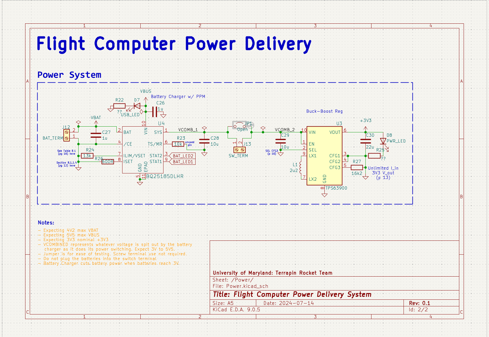
Board 1: STM32 Avionics Board (Simple)
- Platform: KiCad design files
- MCU: STM32H7 (avionics application)
- Complexity: 4 layer embedded hardware board
- Source: Open-source Terrapin Rocket Team design
- Why chosen: Moderate complexity, representative of typical embedded projects
Board 2: STM32L496G-DISCO (Complex)
- Platform: Altium Designer
- Components: 336 total (including 169-pin BGA)
- Layer count: 6 layers
- Dimensions: 70mm x 92mm
- Features: LCD, Audio, Sensors, USB, Arduino headers, multiple power rails
- Why chosen: High complexity, mixed-signal design, real-world reference board
LLM Platforms Tested
- ChatGPT: OpenAI's web interface (accessed via browser, no API calls)
- AI Studio (Gemini): Google's Gemini models via web interface
⚠️ Important Testing Note
We used the free web interfaces for both platforms, not API access. This means we faced context window limitations and couldn't process entire designs in single requests. All data had to be manually prepared and fed to the LLMs in manageable chunks.
How We Prepared the Data
Data Input Methods
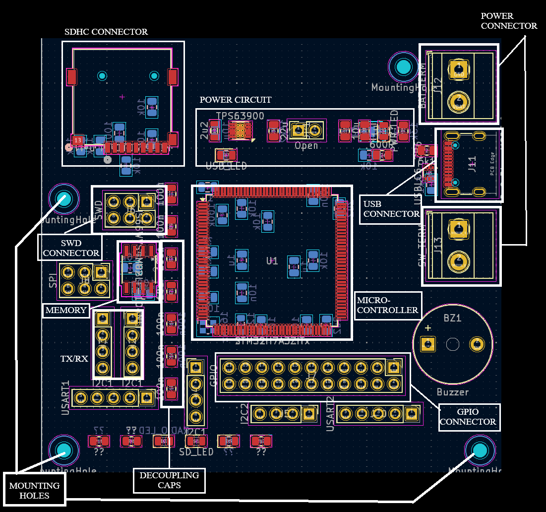
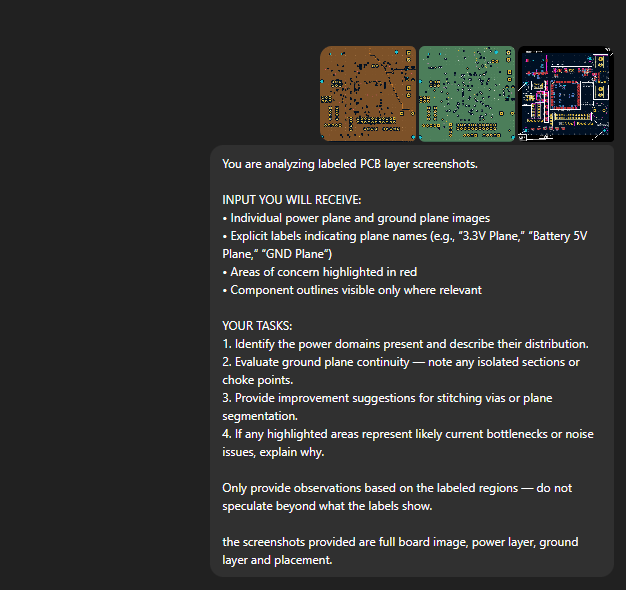
- Schematics: Converted to high-resolution images with clear component labels and net names visible
- PCB Layout: Screenshots of placement with component reference designators and silkscreen data
- Layer Information: Individual layer views with explicit labeling of signal, power, and ground layers
- BOM Data: Component list with part numbers, values, and package information
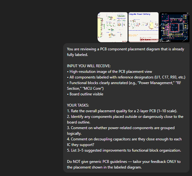
- Labeled Diagrams: Manually annotated placement views showing functional groupings
First key insight from our testing: LLMs need good resolution images to understand the context. The data needs to be extensively labeled and annotated for the models to understand PCB designs. Raw Gerber files, unprocessed screenshots, or complex multi-layer views without explicit labels resulted in complete confusion.
What Actually Worked (With Major Caveats)
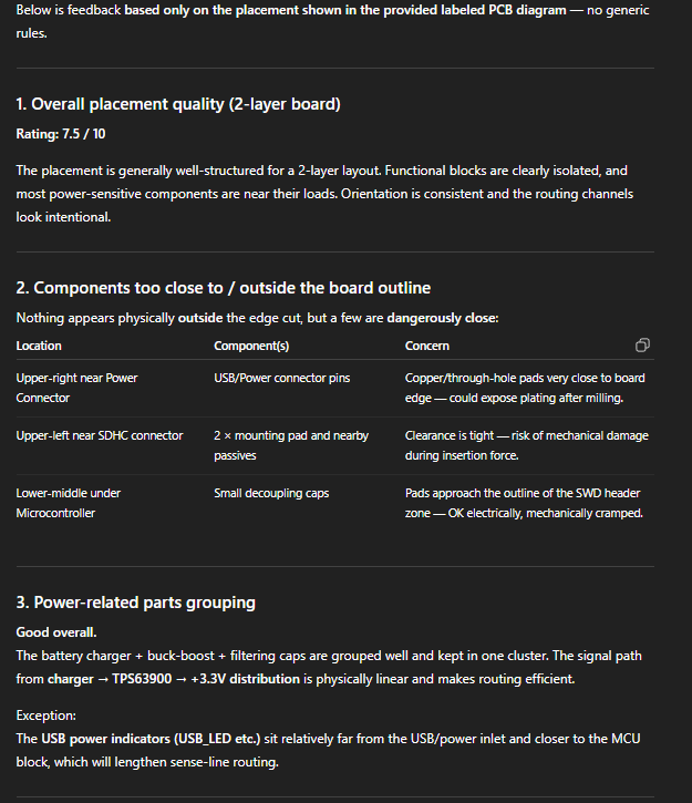
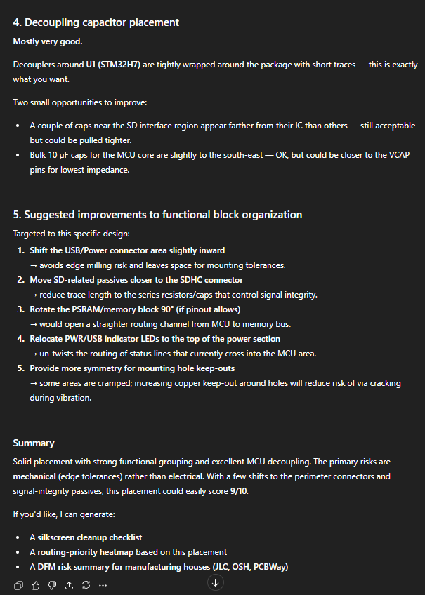
✅ Component Placement Review with Labeled Diagrams
Result: Moderate Success
When we provided clearly labeled placement diagrams showing component groups, reference designators, and functional blocks, both ChatGPT and Gemini could:
- Rate overall placement quality on a subjective scale
- Identify obvious issues like components placed outside board outline
- Recognize when power management circuits were grouped together
- Comment on decoupling capacitor proximity to ICs (when explicitly labeled)
Limitation: This only worked when we spent significant time creating labeled diagrams. The LLMs couldn't extract this information from raw PCB files or unlabeled screenshots.
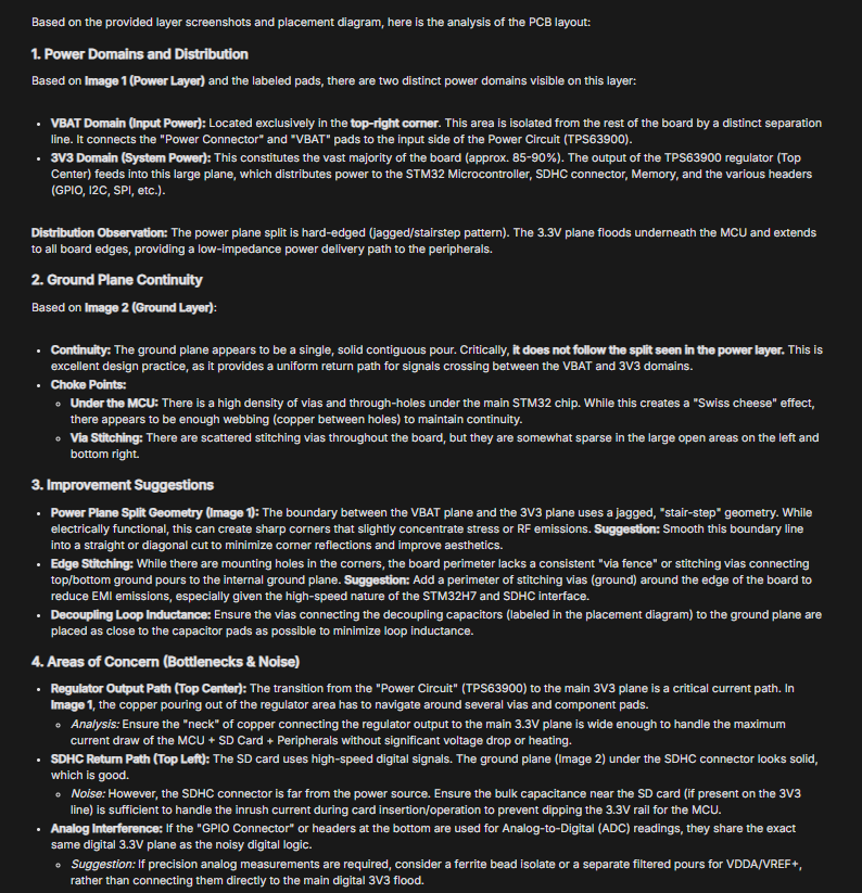
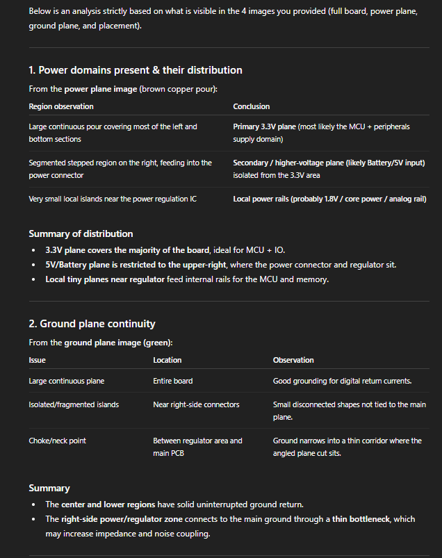
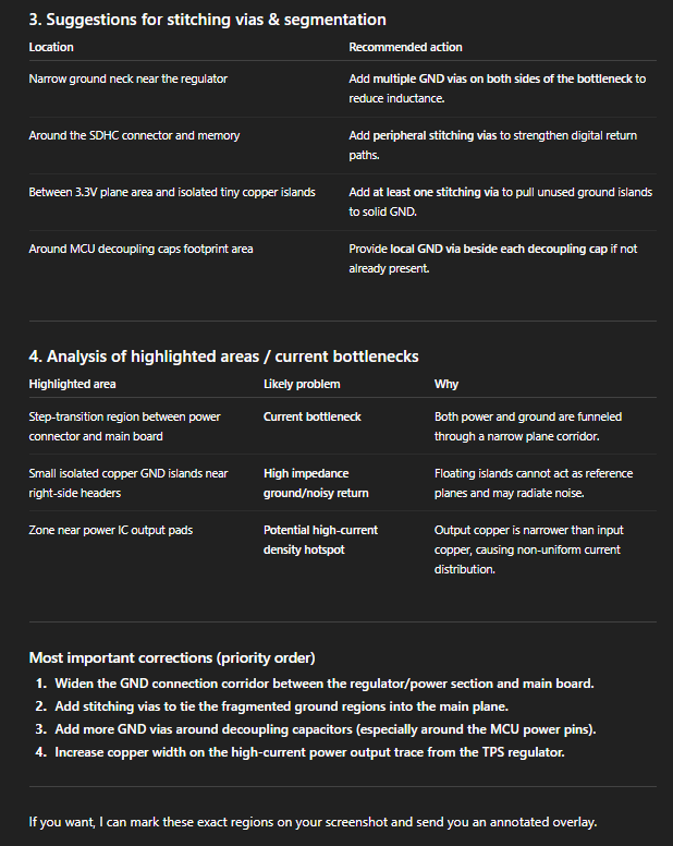
✅ Power Network and Ground Layer Analysis
Result: Worked When Explicitly Labeled
With heavily annotated power plane views, the LLMs could:
- Identify different power domains (3.3V, 1.8V, 5V, etc.)
- Comment on ground plane continuity (when we highlighted problem areas)
Limitation: Without labels explicitly stating "this is 3.3V power plane" or "this is ground plane," the LLMs couldn't distinguish power layers from signal layers.
✅ Design Checklist Generation
Result: Decent But Generic
When asked to generate a PCB design verification checklist, both LLMs produced reasonable lists covering:
- Basic DRC checks (trace widths, clearances)
- Component placement considerations
- General manufacturing guidelines
- Power distribution reminders
Limitation: The generated checklists were far less comprehensive than our existing 200+ point verification framework.
Success Summary
LLMs can provide high-level commentary and general guidance when given heavily pre-processed, labeled data. They work best as "talking textbooks" that can discuss PCB design principles in conversational language, not as verification tools that can analyze raw design files.
What Failed Completely
❌ Top and Bottom Layer Routing Understanding
Result: Could Not Interpret Purpose
Even with labeled bottom layer views, the LLMs struggled to:
- Understand why specific routing patterns were chosen
- Identify return paths for high-speed signals
- Recognize via usage strategies
- Comment meaningfully on routing quality
Why it failed: Routing analysis requires understanding of 3D spatial relationships and electromagnetic principles that text-based LLMs cannot reason about effectively.
❌ Spatial Reasoning and Geometric Relationships
Result: Fundamental Limitation Identified
This was the most critical failure. LLMs could not:
- Calculate distances between components accurately
- Check for overlaps between component outlines
- Understand trace routing paths in 2D space
- Reason about via placement locations
- Identify spatial conflicts or clearance violations
- Measure or verify component spacing
Why it failed: LLMs are trained on text and process visual information by converting it to tokenized representations. They lack genuine geometric reasoning capabilities.
❌ PCB Trace Width Prediction and Verification
Result: Too Primitive for Practical Use
When asked to verify if trace widths were appropriate for current requirements:
- Could not measure actual trace widths from images
- Could not calculate required widths based on current
- Could only provide generic textbook formulas
- Could not identify which traces were undersized or oversized
Why it failed: Requires precise geometric measurement combined with electrical calculations—something LLMs cannot do without external computational tools.
❌ Dense Board Analysis (STM32L496G-DISCO)
Result: Testing Abandoned as "Way Too Much"
When we attempted to analyze the 336-component L496G-DISCO board:
- Context windows couldn't handle the full board data
- Breaking into chunks lost critical spatial relationships
- LLMs became confused by component density
- Responses became increasingly generic and unhelpful
Why it failed: Complex boards exceed the practical limitations of LLM context windows and spatial reasoning capabilities. We stopped testing on this board after recognizing it was futile.
⚠️ When We Stopped Testing
After discovering the above failures, we discontinued testing and did not do a deep dive of the STM32L496G-DISCO board. We thought perhaps our approach was wrong—maybe we should be using a KiCad MCP (Model Context Protocol) server, which can help query the database with natural language.
We explored several MCP implementations, including mixelpixx-kicad-pcb-designer. However, we found significant limitations with the MCP approach:
- No inherent mechanical or enclosure context. Which specific parts are "must be on edge" versus "nice to have near edge"? How should these types of boards be designed?
- Functional placement understanding is limited. Can it generate power trees and understand how power flow should work? Can it properly group components into functional blocks?
- Limited physics understanding. The fundamental limitations in spatial reasoning and physical constraints remain even with MCP integration.
MCP appears to be the right effort, but the underlying models need to advance significantly before the full value of MCP can be realized for PCB design automation. As a note, Altium also has an MCP server available, with similar capabilities —but the fundamental model capabilities remain the bottleneck.
Honest Conclusions: Where LLMs Stand Today
What We Learned
✅ LLMs are great in communicating with natural language.
For engineers learning PCB design or needing to discuss design principles, LLMs provide value as conversational interfaces to technical knowledge. They can explain concepts, discuss trade-offs, and provide general guidance.
✅ LLMs Can Generate Documentation and Checklists
For creating design review checklists, generating documentation templates, or drafting design rationale documents, LLMs can accelerate work. The output requires engineering review but provides a useful starting point.
❌ LLMs Cannot Replace Design Verification Tools
LLMs cannot perform the geometric measurements, electrical calculations, and rule checking that constitute the majority of PCB verification work. They lack the spatial reasoning and computational capabilities required for these tasks.
❌ LLMs Are Not Time-Savers for Verification
The extensive data preparation required to make PCB designs understandable to LLMs takes longer than traditional manual review by an experienced engineer. Even with perfectly prepared data, LLMs can only verify a small fraction of what needs checking.
❌ Complex Boards Exceed LLM Capabilities
As board complexity increases (more components, more layers, denser routing), LLM effectiveness decreases rapidly. Our 336-component board was simply too complex for meaningful LLM analysis, even with extensive data preparation.
Conclusion
The path forward isn't general-purpose LLMs trying to understand PCB designs—it's purpose-built AI tools that integrate with EDA platforms and can access structured design data directly. We predict a future where multiple agents would be communicating with other specific agents to verify the design objectives. We had already listed this in our blog here.
There is a lot of work being done to make LLM execute multiple tasks simultaneously. Here is one such study: https://arxiv.org/abs/2511.09030. This paper introduces MAKER, a system that lets large language models reliably execute over one million dependent steps in a single task with zero errors. The authors aggressively decompose a big problem into many tiny subtasks, each handled by a specialized "micro-agent."
They use a strong modular structure plus a multi-agent voting scheme for error correction at every step, so local mistakes get caught and fixed before they propagate. A YouTube video breaks down this paper in more detail:
Could this be the answer for our issues? We don't know yet.
Want to know more about how we use AI with PCB design?
Check other blogs where we frequently talk about integrating AI with PCB. We cover boards designed using same AI PCB automation and PCB autorouting algorithm in Altium, Cadence, KiCad and other tool series.
Visit Blogs Request Technical Discussion