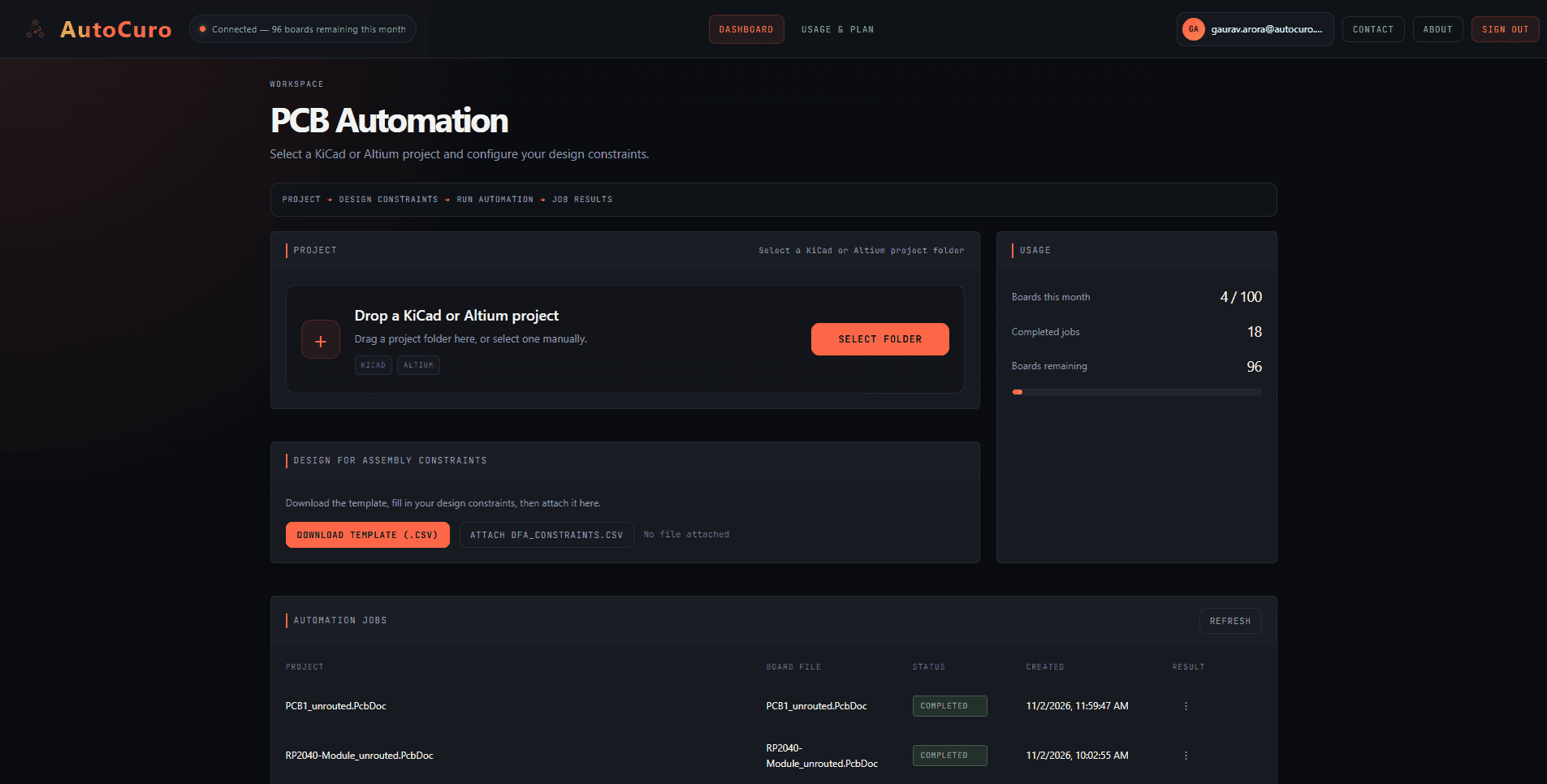
The AutoCuro desktop app runs component placement and routing for KiCad, Altium Designer and Cadence Allegro boards on your own computer. This post walks through what the app does, what you need to give it, and a routed 4-layer board, including the parts that still need an engineer.
1. Why a Desktop App?
Our browser-based routing beta routes boards that are already placed, accepts up to four copper layers, and may publish submitted boards and routed results in a public GitHub repository. That works for open-source designs, but most commercial boards cannot be shared.
The desktop app is for those boards. It runs on your own computer, it handles component placement as well as routing, and your schematic and layout files stay on your machine rather than being uploaded to our servers.
To be precise about what does leave your machine: the app needs internet access for licensing, and it sends high-level metadata about design parameters and usage statistics. This metadata does not include your design files. The details are in our Terms and Conditions (sections 5.1 and 5.2).
2. Supported Tools and System Requirements
The app works alongside the PCB design tool you already use. You prepare the design in your tool, run placement and routing in the app, and review the result back in your tool.
- Altium Designer (version 23 and later): you export the schematic and constraints from Altium, run placement and routing, then import the results back into Altium for review and refinement.
- Cadence Allegro (version 17 and later): you export schematics, constraints and the board outline from Cadence, run placement and routing, then bring the results back into the Cadence environment.
- KiCad (version 10): the output is a standard KiCad PCB file that you open and edit in KiCad as usual.
Minimum System Requirements
- Windows
- 8-core CPU
- 16 GB RAM
- Internet access for licensing
- Your PCB design tool (KiCad, Altium Designer or Cadence) installed for file import and export
More complex designs benefit from additional CPU cores and RAM.
3. What You Provide
The app works from your schematic, not just the netlist, so it needs the schematic files alongside the board file.
Required Inputs
- Schematic files: for example, .SchDoc for Altium Designer, .sch for Cadence or .kicad_sch for KiCad. These carry the connectivity and hierarchy the app uses to understand the circuit.
- Board file: with the board outline defined and the component footprints placed outside the outline.
- Design rules file: track widths, clearances, via sizes and drill specifications, and layer stackup, supplied through an external configuration document.
Optional Inputs
- Pre-placed components: you can fix certain connectors, mounting holes or specific ICs before running automation. The app keeps your placements and places the remaining components around them.
- Keep-out zones and mechanical constraints.
The app does not create the board outline, and it does not decide your design rules. Both come from you. Set the rules to match your layer stackup and your fabricator's capabilities before running the app; on high-speed boards, this includes the trace widths and spacing for impedance-controlled nets and differential pairs.
4. The Dashboard and Workflow
You start by selecting the design folder that holds your schematic and board files. A step-by-step panel then takes you from folder selection through to Gerber generation.
Placement, routing and Gerber generation each produce their own output, and you can rerun any of them without repeating the whole cycle. Two controls matter most:
- Placement generates component placement and routing in a single pass.
- Initiate Routing takes the placement already on the board and routes it, without moving any components.
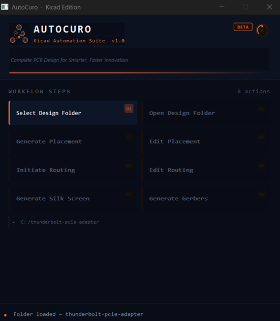
This separation lets you accept the automated placement as it is, adjust it before routing, or route a placement you made yourself.
5. Checks at Each Stage
The app reports on the design as it goes, so problems surface before you spend time on a full run.
- Netlist errors: netlist integrity and connectivity are checked before processing begins.
- Library mismatches: inconsistencies between components, footprints and libraries are flagged.
- Placement scores: placement quality is scored against the design rules.
- DFA/DFM reports: Design for Assembly and Design for Manufacturing reports are generated with the output.
- Routing scores: routing quality and completion are reported.
These reports are a structured starting point for review. They do not replace your own design rule check, your manufacturer's checks or an engineer's sign-off.
6. Automated Placement
Placement quality decides how well a board can be routed, so the app reads the schematic first and identifies functional blocks before placing anything.
- Functional grouping: related components are kept together. Power circuits stay with power circuits, interface components cluster near their connectors, and MCU support parts are arranged around the processor.
- Decoupling capacitors are placed close to the power pins they serve.
- Crystal oscillators are placed with their load capacitors.
- Both board sides can be used. Our STM32MP257F-EV1 case study in Altium Designer shows the automated placement next to ST's publicly available reference placement, so you can compare the two directly.
Placement is the area we are still improving most. On every board we have documented, the automated placement was reviewed and adjusted by an engineer.
7. Automated Routing
After placement, the router works through the board in this sequence:
- Power plane decision
- Power supply fanouts
- Stackup selection, if you have not supplied one
- Differential pair routing strategy
- Via optimisation
- Trace routing
- Cleanup
If the app selects the stackup, check it against your manufacturer's available stackups before you rely on it.
Specific Routing Behaviour
- Differential pairs are identified from the schematic net naming and routed as pairs. Where a pair's polarity is swapped in the schematic, the router adds a crossover rather than requiring a manual net swap.
- BGA escape routing is generated with pin-aligned trace exits, for any BGA pitch your design rules allow.
- Bus length matching is applied to parallel buses running above 50 MHz.
- Layer assignment follows your constraints file when one is provided, rather than a fixed stackup assumption.
- Via reduction: the router avoids extra layer changes where a signal can continue on the same layer.
- Power and ground nets are routed with wider traces, and dedicated power layers get continuous plane polygons.
Track widths, spacing and clearances all come from your design rules file. The router follows those rules; it does not choose them for you.
8. Post-Route Checks and Outputs
After routing, the app looks for issues that a standard DRC does not catch. We describe these in more detail in PCB Design Errors Your DRC Tool Won't Catch.
- Critical buses routed inconsistently across layers
- Clock net stubs
- Differential pairs crossing reference-plane voids
- Power-plane splits that interrupt a signal's return path
- Floating vias
- Pads sitting over copper voids
Some of these are corrected on the routed board, and others are flagged for you to review. They are prompts for engineering review, not a substitute for signal integrity analysis.
Outputs
- The placed and routed board in your tool's native format, ready to open and refine
- DFA and DFM reports
- Gerber files, generated once you approve the design for release
9. Board Walkthrough: Glider E-Paper Controller
To show a full run, here is Glider (revision R1.3), an open-source e-paper display controller board designed in KiCad. It packs a lot of routing into 90 × 80 mm: a Xilinx Spartan-6 FPGA in a 256-ball BGA, a 16-bit DDR3L memory, an STM32H750 microcontroller, an HDMI receiver, a USB-C input with DisplayPort alternate mode, an LVDS bridge and the e-paper panel power supplies.
- Copper layers: 4 — signals on top and bottom, a ground plane on In1.Cu and split power planes on In2.Cu
- Components: 379, with 1,821 pads
- Nets to route: 356, including 41 differential pairs and the FPGA-to-DDR3L interface
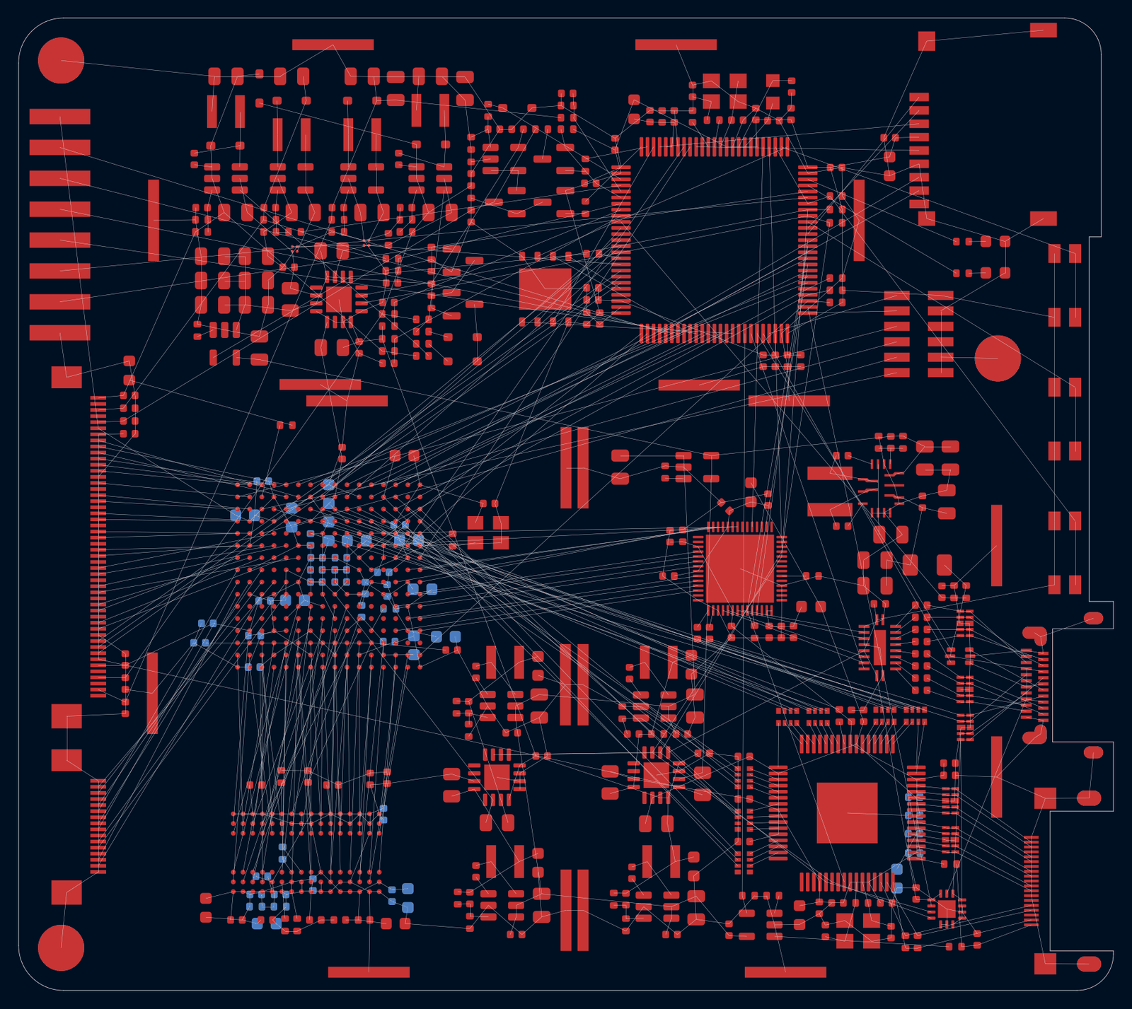
Step 1: Input Board
The run started from a placed board with no copper routed. Every connection the router had to make is still a ratsnest line: 1,225 unrouted connections in total, most of them concentrated around the FPGA, the DDR3L memory and the video interfaces on the right-hand edge.
Step 2: Routing
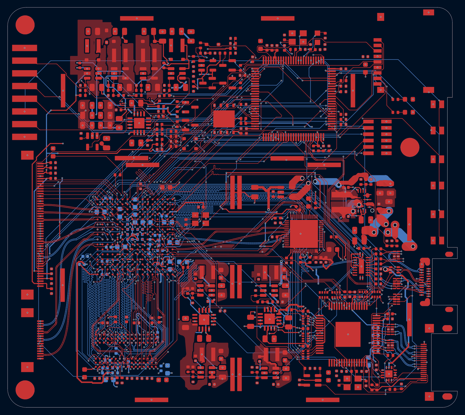
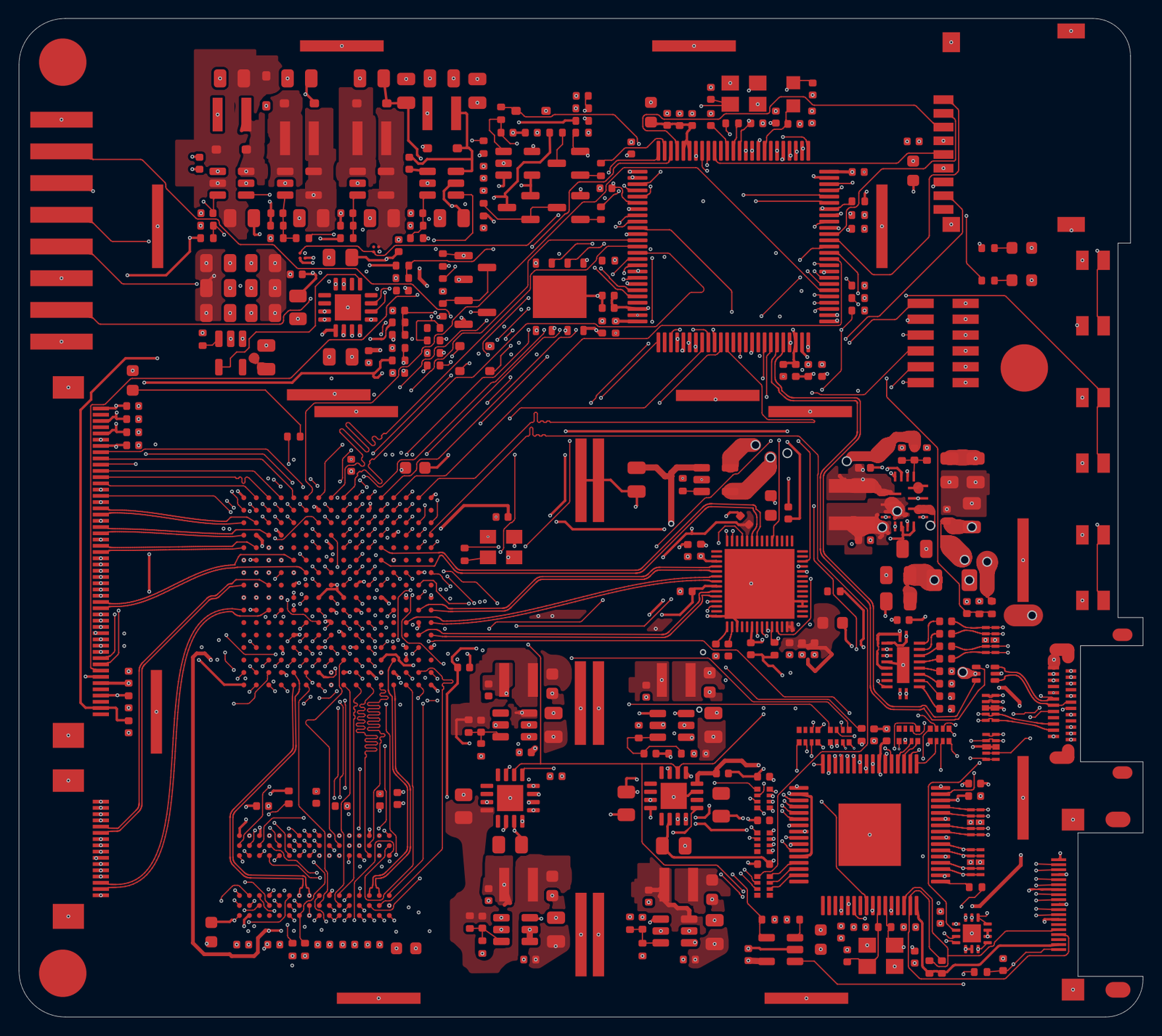
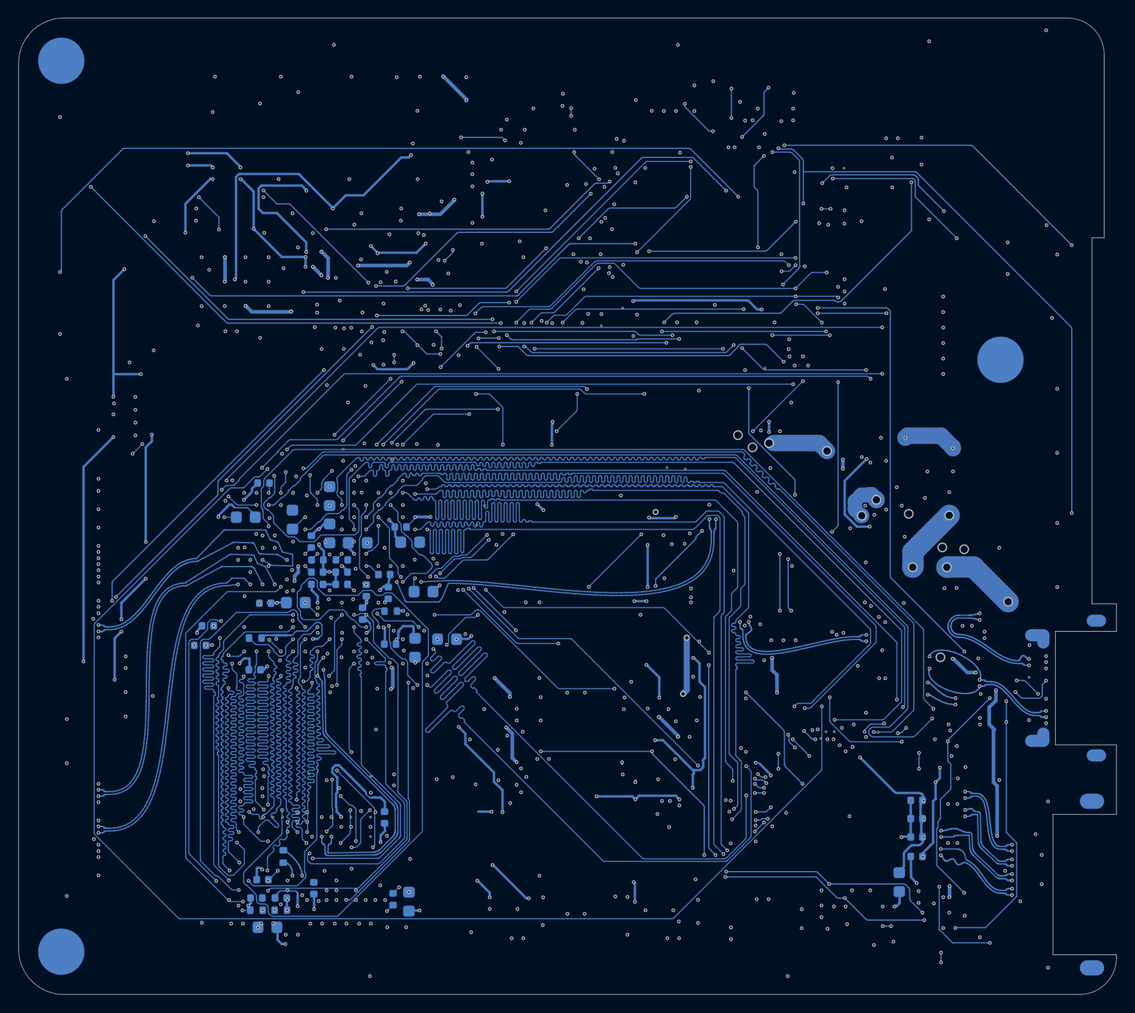
The board was routed with Initiate Routing, so no components moved. The router handled the FPGA BGA fanout, the DDR3L interface, the differential pairs, layer assignment and via placement, and generated the ground and power planes.
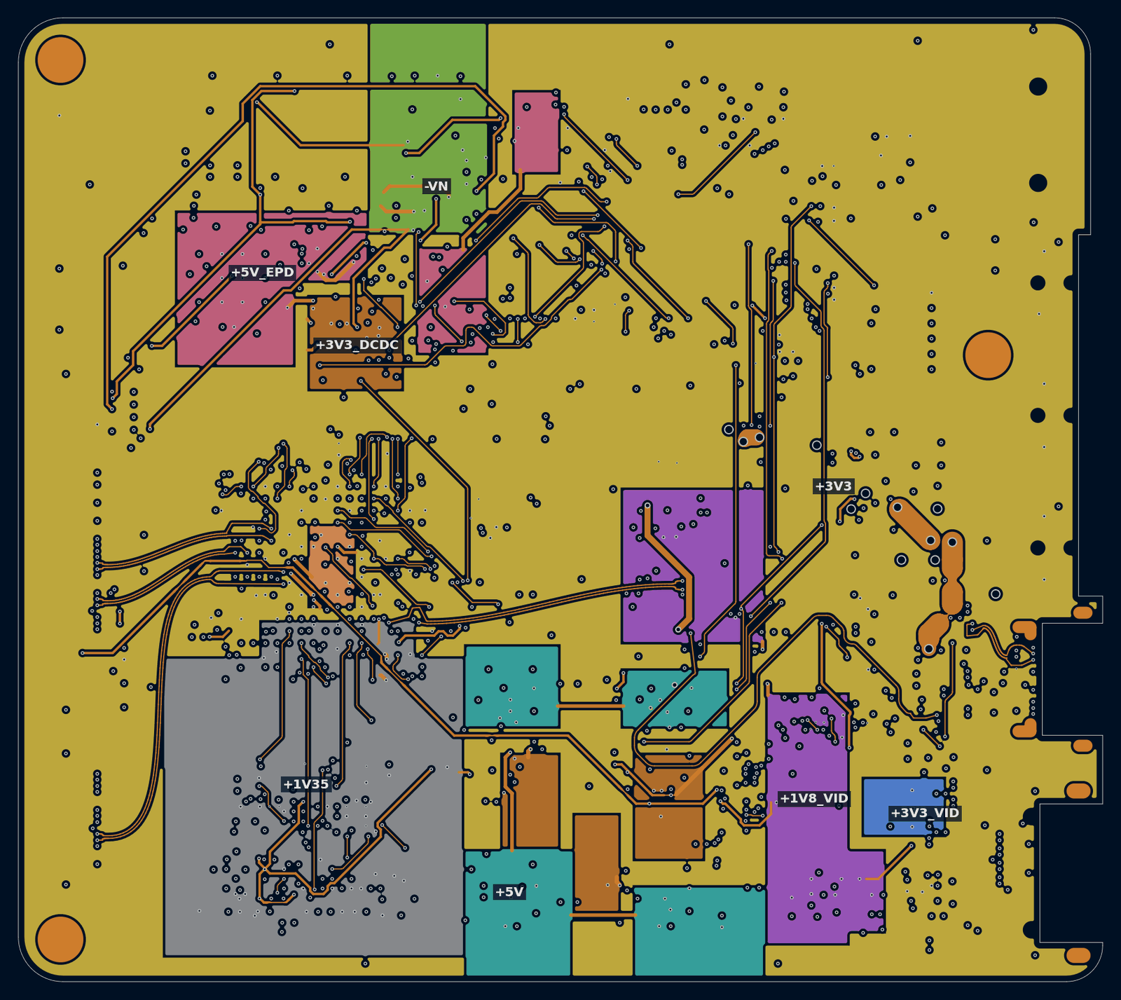
Ground and Power Planes
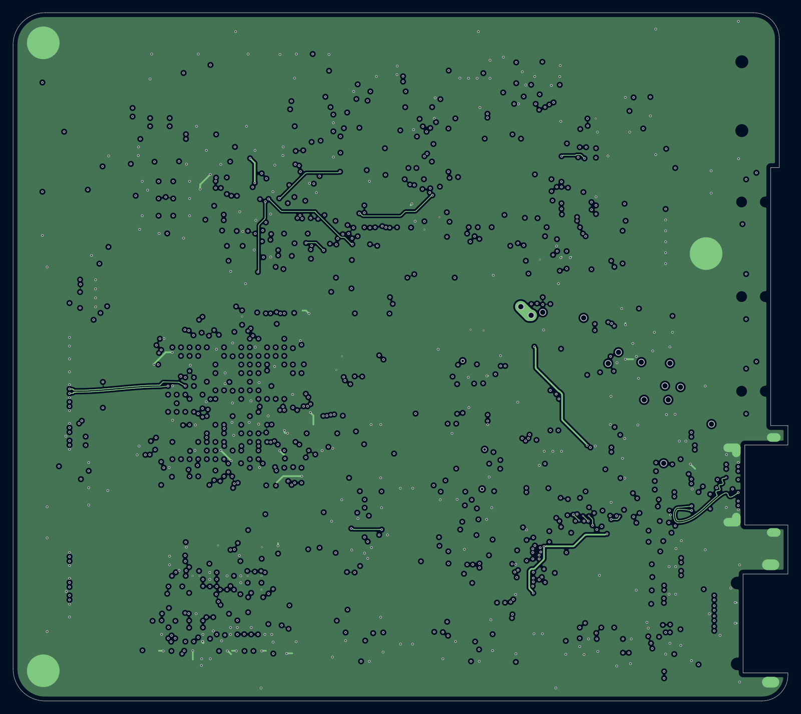
In1.Cu was kept as a near-continuous ground plane, giving the signals on the top layer an unbroken return path. In2.Cu was split into plane regions for nine supply nets, including the FPGA core (+1V2_FPGA), the DDR3L supply (+1V35), the video supplies (+1V8_VID and +3V3_VID) and the e-paper supplies (+5V_EPD and -VN).
DDR3L Routing and Length Matching
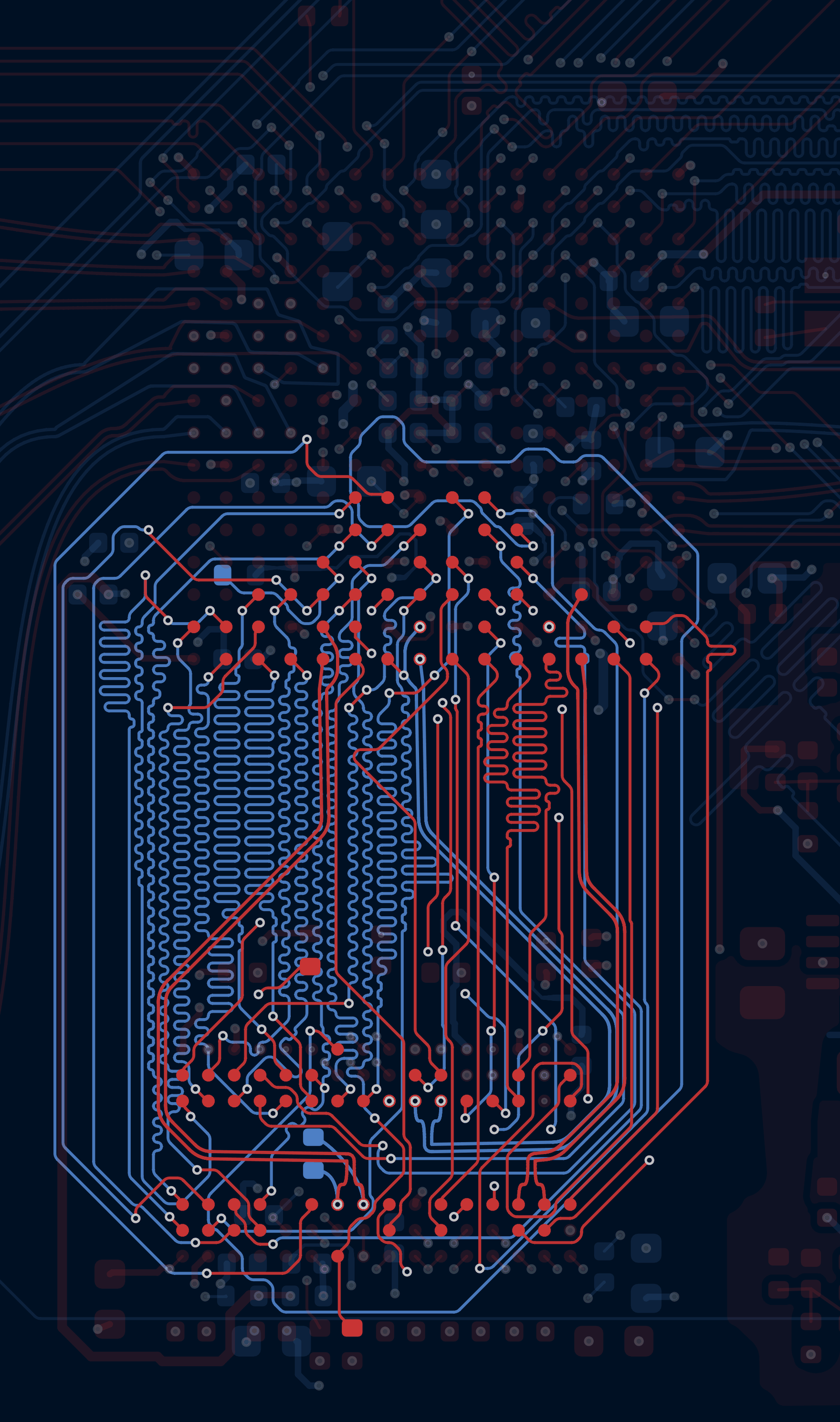
The DDR3L interface runs between the FPGA and the memory directly below it. Most data lines stay on the top layer, while the address, bank and command lines drop to the bottom layer, where the router added serpentine tuning to bring them towards a common length. Nine of those nets landed within 0.2 mm of a 34.4 mm target.
Differential Pairs
The router identified 41 differential pairs from the schematic net names and routed them as coupled pairs, including the HDMI TMDS lanes, the DisplayPort lanes from the USB-C connector, the USB 2.0 pair, the LVDS links and the e-paper data lanes. The four HDMI TMDS pairs came out within 0.04 mm of intra-pair skew.

Step 3: Results
Routing Results for This Board
Lengths are measured as copper track length in the routed KiCad file, excluding via barrels.
Of the 23 nets that are not complete, 16 are power or ground nets with a few connections still to be made to their planes or pours. The other seven are signal nets, including three differential pairs: one DisplayPort lane, the SBU pair on the USB-C connector and one LVDS pair. These need manual completion. Manual refinement time for this board has not yet been measured.
10. What Still Needs an Engineer
The routed board is a starting point. Before any board goes to fabrication, it needs an engineer's review and your normal checks. On the boards we have documented, these tasks still fell to the engineer:
- Defining the board outline and setting appropriate design rules
- Completing traces the router did not finish
- Removing extra vias and cleaning up traces
- Checking and correcting differential pair spacing
- Fine length tuning within each differential pair, for example on DisplayPort, LVDS and e-paper data lanes
- Adjusting power planes
- Refining component placement, particularly decoupling networks, crystals and connector alignment to board edges
For another documented example of this work on a complex board, see our STM32MP257F-EV1 case study in Altium Designer.
11. Desktop App vs. Browser Beta
| Browser Beta | Desktop App | |
|---|---|---|
| What it does | Routing only. Components must already be placed. | Placement and routing, run together or separately, plus Gerber generation. |
| Input | A placed board file: .kicad_pcb, .PcbDoc or .brd. | Schematic files, a board file with the outline defined, and a design rules file. |
| Copper layers | Up to four. | Our published case studies include 6-layer boards. |
| Where your files go | Uploaded for processing. Boards and results may be published in a public GitHub repository. | Stay on your machine. Licensing and high-level metadata only. |
| Reports | Routing report, emailed with the routed board. | Netlist and library checks, placement and routing scores, DFA/DFM reports. |
| Access | Free, two boards per month, GitHub sign-in. | Licensed. Contact us for a demonstration and pricing. |
12. Request a Demo
If you have a board you cannot put through a public tool, we can run a demonstration with your own design or a sample project. We will walk through the workflow on your type of board and discuss whether automation is a good fit for it. There is no commitment required.
Write to us at admin@autocuro.com. If your board is open source, already placed and has four copper layers or fewer, you can also try the free browser routing beta.