Why This Board Is a Meaningful Test
The STM32MP257F-EV1 is STMicroelectronics' evaluation platform for the STM32MP257FAI3 microprocessor. It is not a simple breakout board. It is a dense, mixed-signal design with multiple high-speed interfaces, a dedicated power management IC, and several communication protocols sharing a constrained board area.
The processor itself comes in a TFBGA436 package — 436 balls at fine pitch. Around it, the board integrates DDR4 memory, three Gigabit Ethernet ports with Time-Sensitive Networking support, CAN FD interfaces, USB Type-C, LVDS and DSI display outputs, a camera interface, and PCIe. Each of these interfaces has its own routing constraints: impedance targets, differential pair requirements, length matching tolerances, and keep-out considerations.
For a human layout engineer, this board represents a minimum of three weeks of focused work from schematic handoff to DRC-clean layout. The density of the BGA fanout, the number of competing differential pair groups, and the power distribution complexity make it a design where every placement decision affects downstream routability.
We chose this board specifically because its design files are publicly available from ST, which means every claim in this case study can be verified against the original reference design.
Board Specifications
| Parameter | Detail |
|---|---|
| Processor | STM32MP257FAI3 — Dual Cortex-A35 (1.5 GHz) + Cortex-M33 (400 MHz) |
| Package | TFBGA436 (18 mm x 18 mm) |
| Memory | DDR4 (32-bit bus), eMMC v5.0, sNOR Flash |
| PMIC | STPMIC25 (dedicated power management IC) |
| Ethernet | 3x Gigabit Ethernet with TSN support |
| Display | LVDS + DSI connectors |
| Camera | CSI connector |
| USB | 1x USB Type-C DRD + 2x USB Host Type-A |
| Other Interfaces | 2x CAN FD, mini PCIe, microSD, Raspberry Pi GPIO header, mikroBUS |
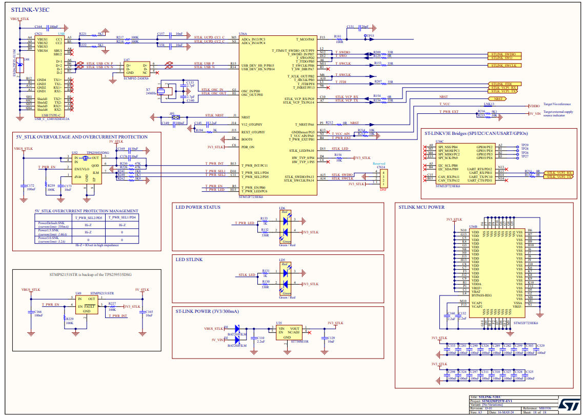
| Debug | On-board STLINK-V3EC |
| Design Tool | Altium Designer |
| Reference | ST Product Page |
Design Challenge
The STM32MP257F-EV1 presents several simultaneous routing challenges that make it a demanding board for any automation system. Each interface on this board carries its own set of constraints, and those constraints compete for the same routing channels and board layers.
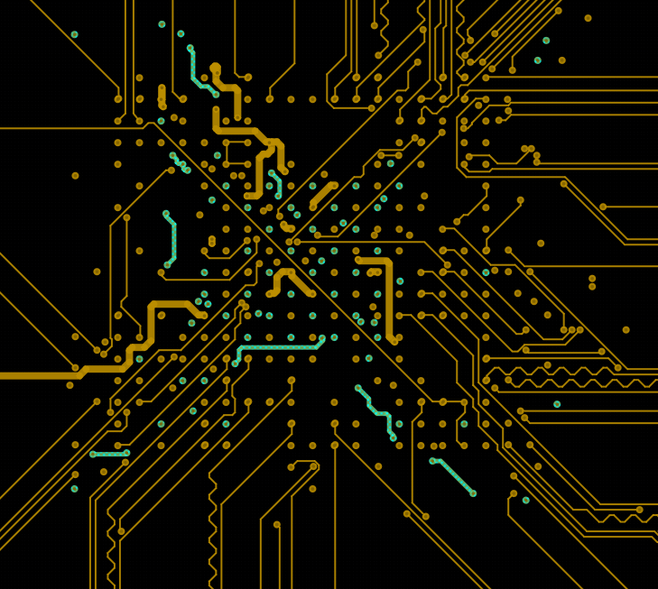
📍 BGA Fanout at Fine Pitch
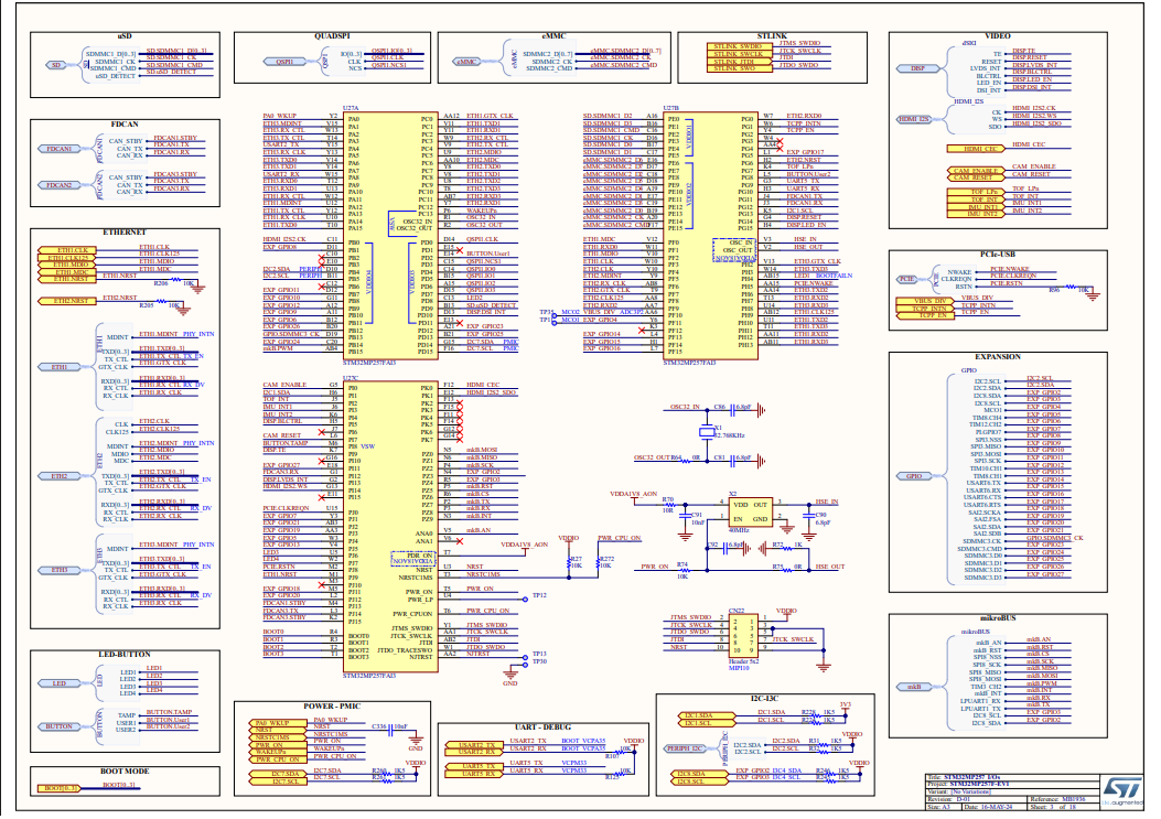
The STM32MP257FAI3 is packaged in a TFBGA436 — 436 balls at fine pitch across an 18 mm × 18 mm body. Routing escape from this package requires careful via placement and layer transition planning to avoid clearance violations while maintaining signal continuity across all interfaces simultaneously.
⚡ DDR4 Length Matching Requirements
DDR4 data buses require tight intra-group and inter-group length matching tolerances. The data strobe (DQS) and clock pairs must be matched within the memory controller's timing budget. These constraints directly influence where memory components can be placed and how routing channels through the BGA escape area are allocated.
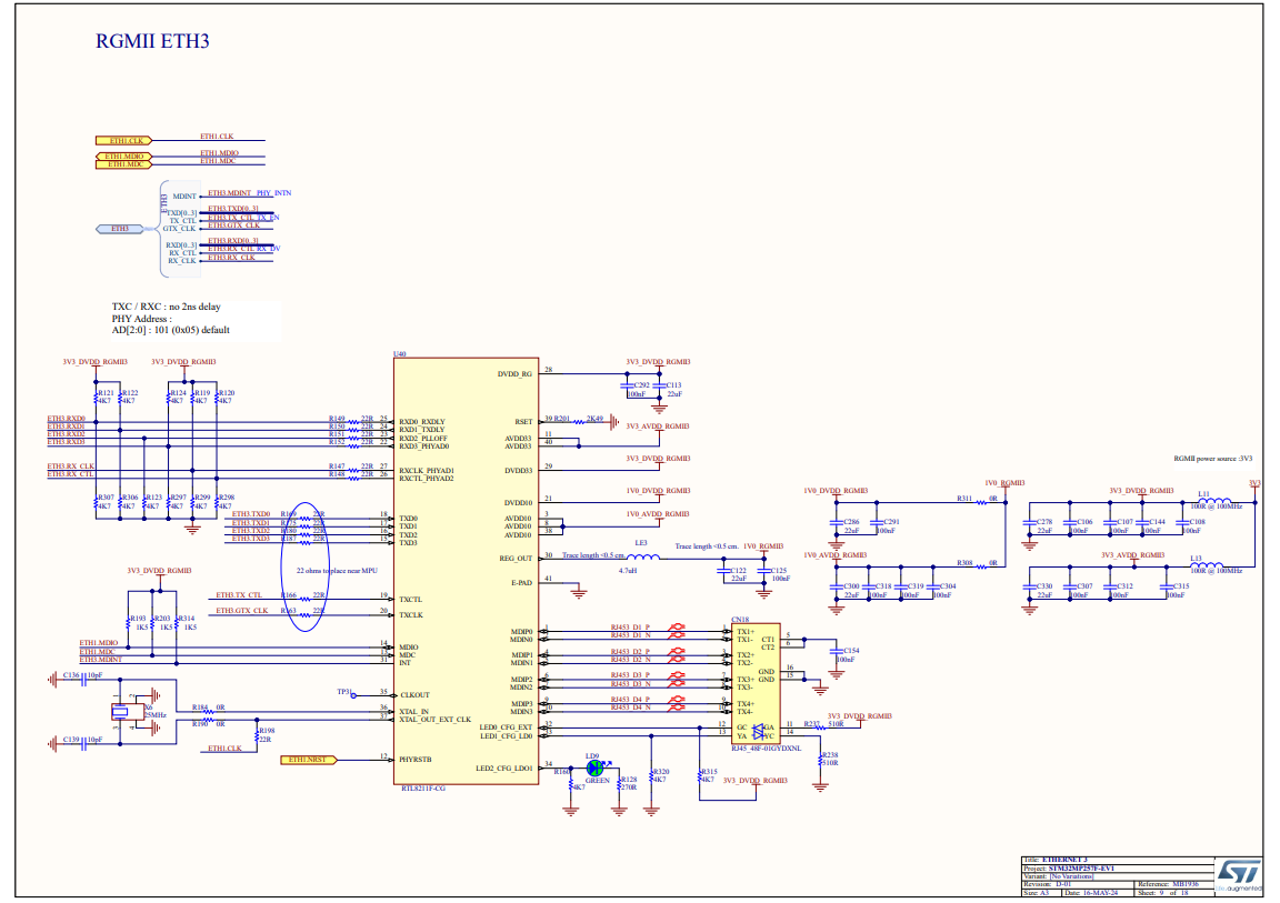
🔌 Triple Gigabit Ethernet Differential Routing
Three independent Gigabit Ethernet ports, each with TX/RX differential pairs and associated magnetics, require routing to their respective connectors without crosstalk between channels. Pair spacing consistency and isolation between the three independent PHY circuits are primary routing concerns.
🎯 Mixed-Signal Interface Density
USB Type-C, LVDS, DSI, CSI, PCIe, and CAN FD all share the board simultaneously. Each interface has different impedance targets and length requirements. Managing all of these across a constrained board area — without the routing channels for one interface degrading another — is the central challenge this board presents.
⚙️ Power Distribution Complexity
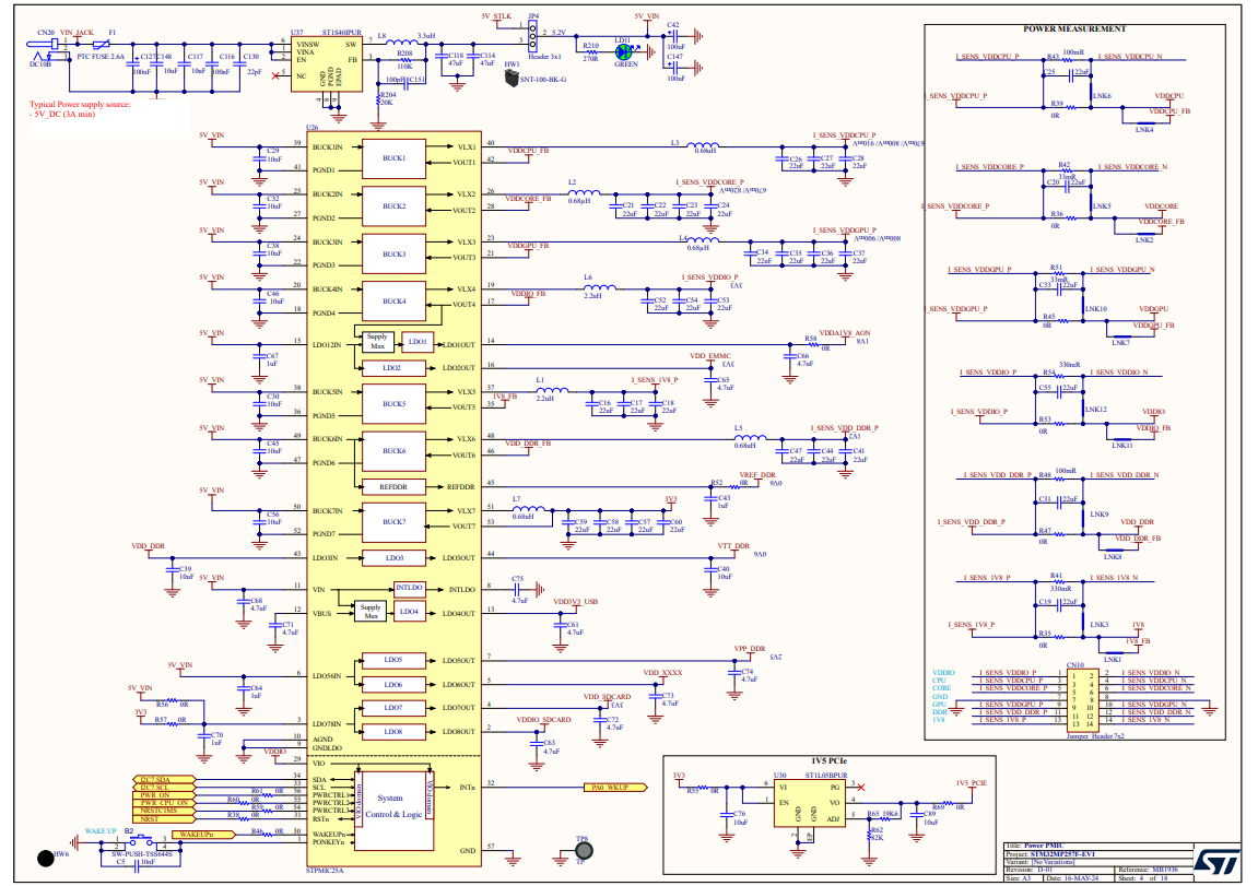
The STPMIC25 generates multiple output rails for the processor, DDR4, and peripheral interfaces. Power plane splits, decoupling placement, and current return path continuity all interact with the signal routing strategy and must be considered from the first placement decision.
Automation Approach
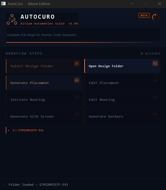
The automation runs locally as a desktop application for Altium Designer. The engineer selects the Altium project folder containing the schematic and board files, and the tool runs placement, routing, or both steps independently from the dashboard.
Schematic-Driven Intelligence
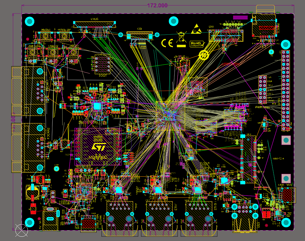
The workflow is structured as a sequential set of steps, from project folder selection through to DRC. The screenshot below shows the AutoCuro · Altium Edition dashboard with the STM32MP257F-EV1 project loaded and ready to process.
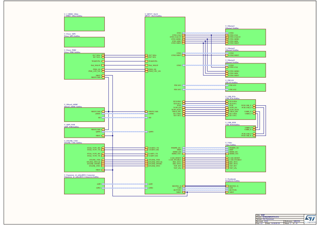
From the schematic, the automation identified the processor and its immediate DDR4 memory bus, the STPMIC25 power management block and its rail assignments, the three Ethernet PHY circuits and their connector associations, the USB Type-C interface, and the display and camera connectors. These functional groupings drive both placement decisions and routing priority ordering.
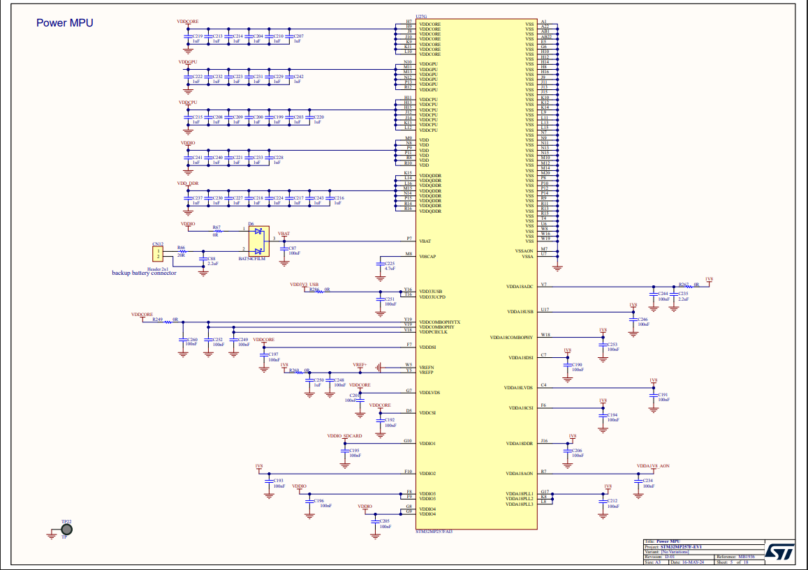
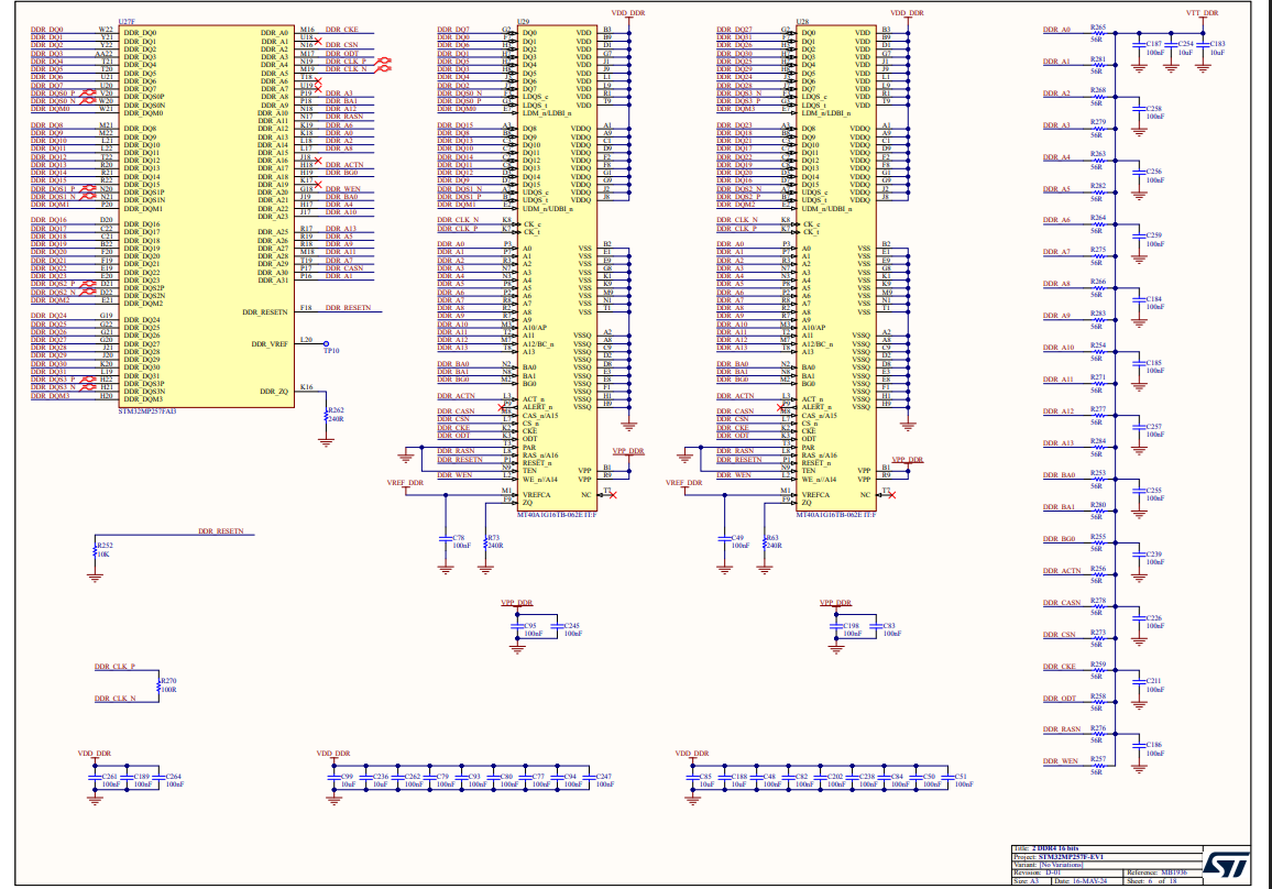
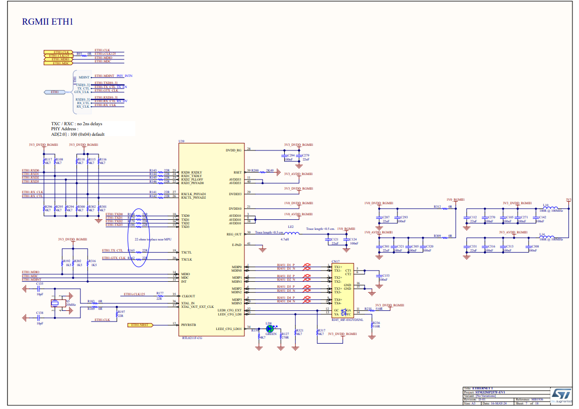
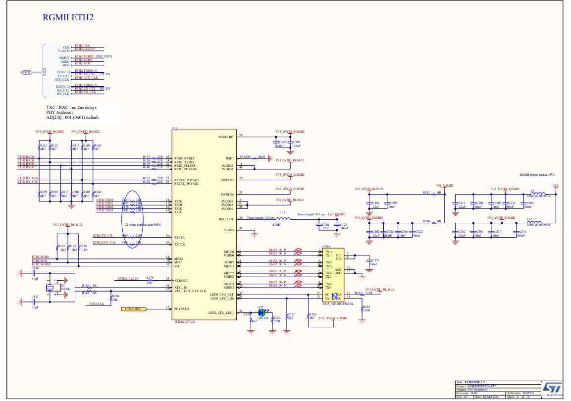
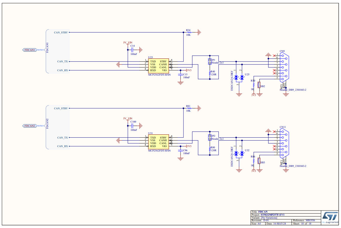
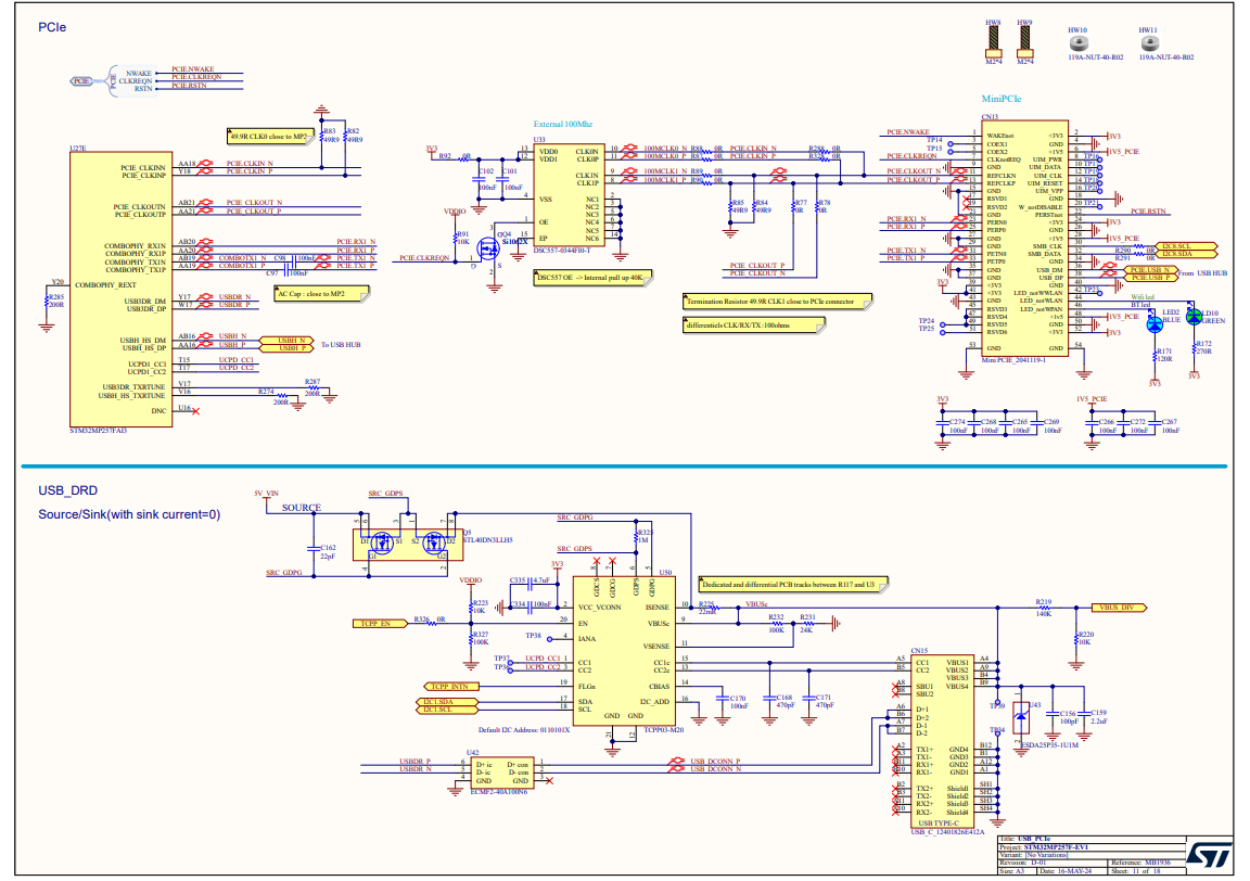
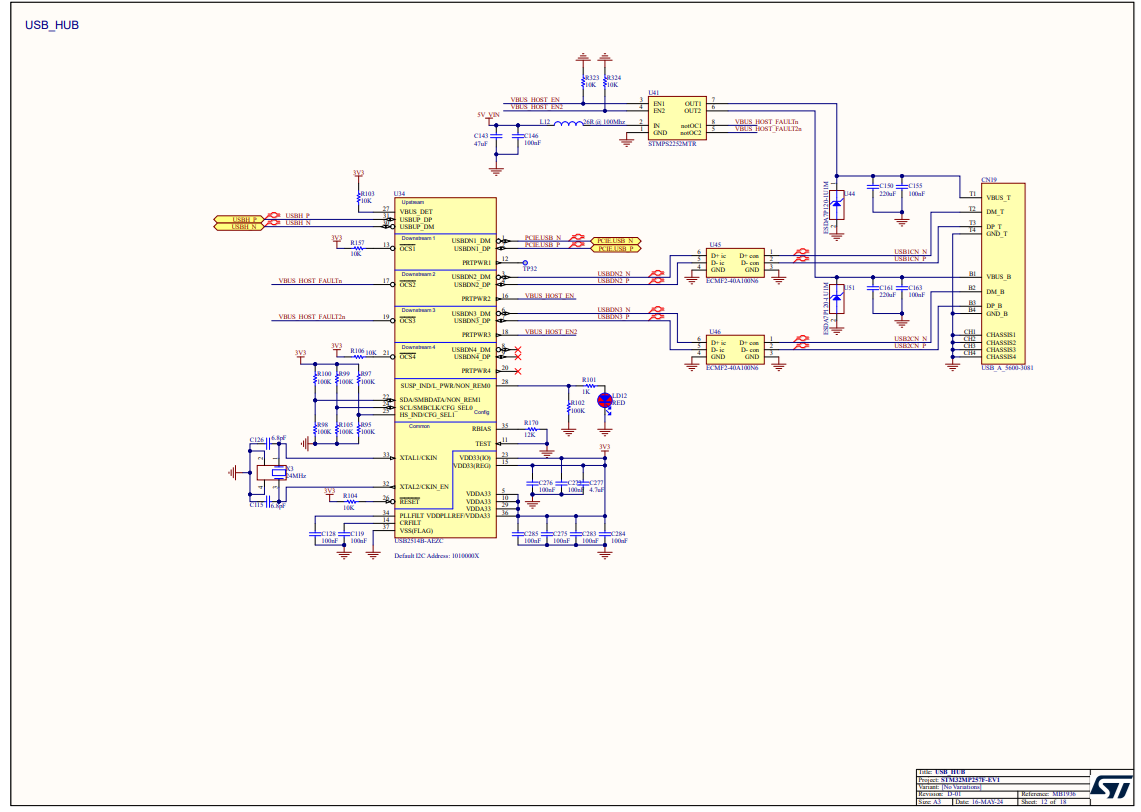
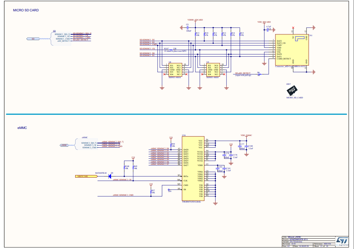
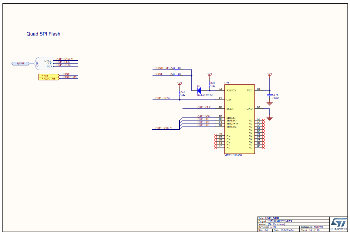
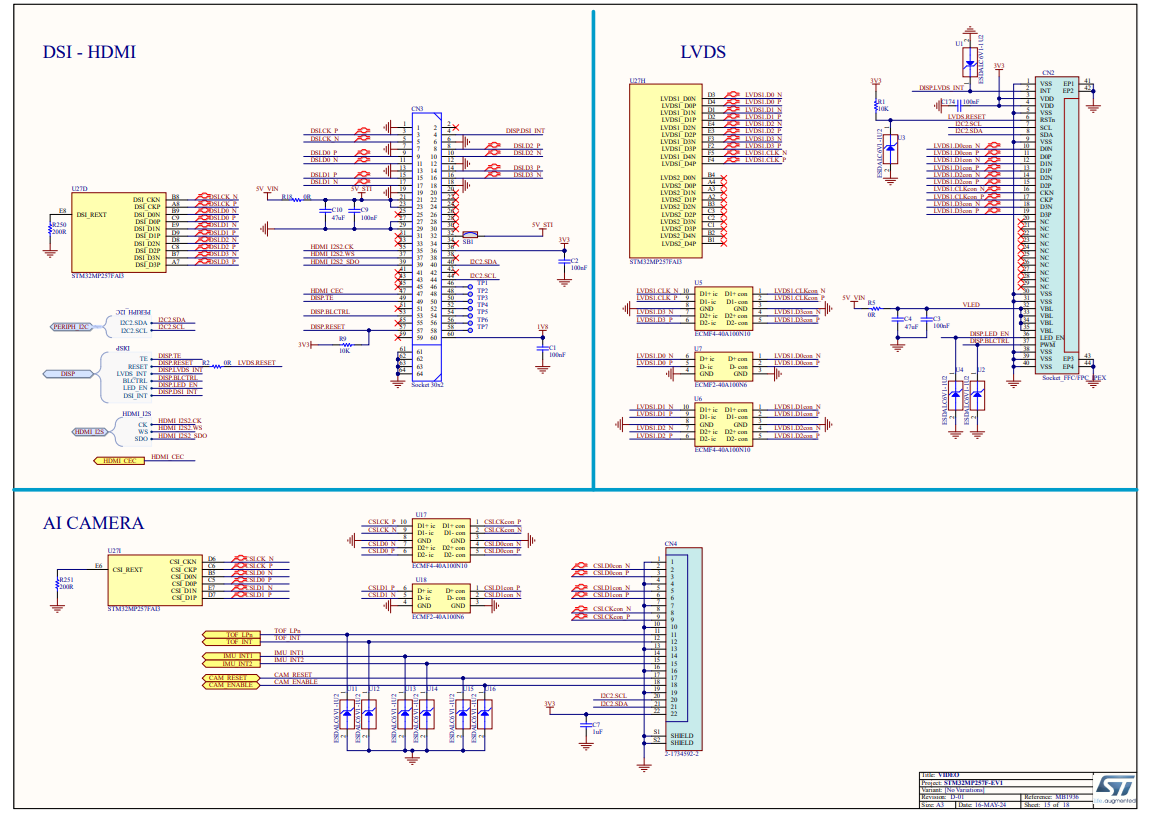
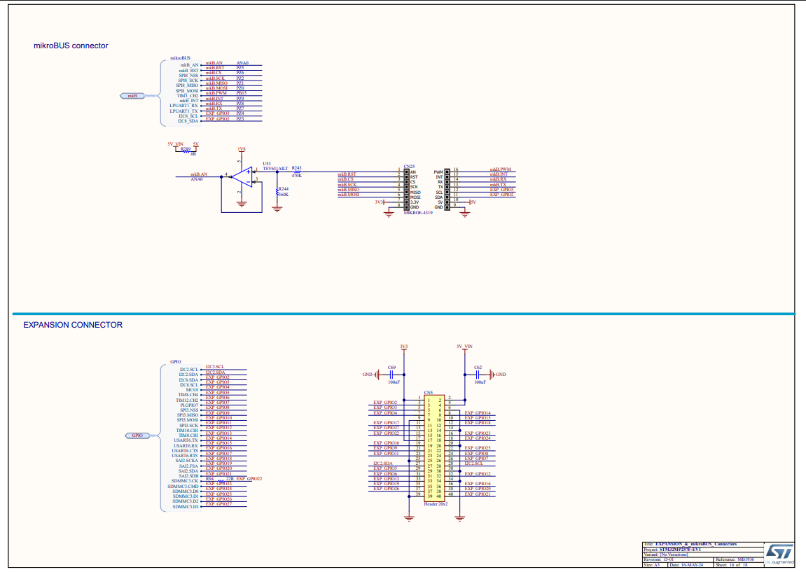
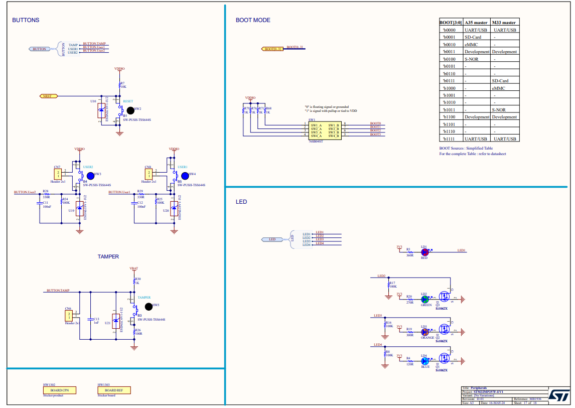
Schematic Pages
Click any schematic page below to expand it.
Placement and Routing Control
The automation gives engineers direct control over which steps to run. Running placement generates component groupings from the schematic analysis. Running routing takes the existing placement as-is and completes signal connections across the configured layer stackup. The two steps can be run together or independently — an engineer can accept the automated placement, replace it with a custom arrangement, or iterate on placement before committing to routing.
Design Setup and Constraints
Before running automation, the following was configured from the reference design documentation and standard design practices:
Input: Altium Project Files
Schematic, component library, footprints, and board outline were prepared in Altium Designer. The automation reads the schematic to understand circuit topology, net connectivity, and component relationships before making placement or routing decisions.
Board Outline and Mechanical Constraints
Board dimensions and mounting hole locations were defined based on the reference design. Connector positions along the board edges were pre-constrained to their mechanical locations.
Layer Stackup
The layer stackup was configured to match the reference design requirements, providing dedicated signal, power, and ground layers appropriate for the interface density on this board.
Design Rules
Track widths, clearances, via sizes, and differential pair spacing rules were set based on the target manufacturer's capabilities. These rules are read from an external configuration that the automation follows during both placement and routing.
Automation Workflow: Step by Step
The automation followed a structured sequence from schematic analysis through to DRC. Each step below describes what the tool did and why.
Step 1: Schematic Analysis and Net Classification
The tool reads the schematic to identify functional blocks: the processor and its immediate peripherals (DDR4 memory, PMIC decoupling), the Ethernet PHY circuits, USB interface components, display connectors, and debug circuitry. Nets are classified by type — power rails, differential pairs, high-speed signals, and general-purpose I/O — so that placement and routing decisions can respect the different requirements of each group.
Step 2: Component Grouping and Placement
Components belonging to the same functional block are grouped together. The STPMIC25 and its associated inductors, capacitors, and feedback resistors are clustered as one power management group. DDR4 memory and its bypass capacitors are placed close to the processor's memory bus pins. Ethernet PHY components are grouped near their respective RJ45 connectors. The tool attempts to minimize trace lengths within each group while keeping routing channels open between groups.
Placement completed in approximately 10 minutes.
Step 3: Routing — Power, Signals, and Differential Pairs
The routing engine works through nets in priority order. Power distribution nets and their return paths are routed first to establish clean reference planes. Differential pairs for DDR4, USB, and Ethernet are routed next with their spacing and impedance constraints. General-purpose signals are routed last, filling the remaining routing channels. The additional differential routing on this board accounted for most of the routing time.
Routing completed in approximately 5 hours.
Step 4: DRC Check
After routing, the design was checked against the configured design rules. The DRC results identified areas that required manual attention — these are detailed in the Manual Refinement section below.
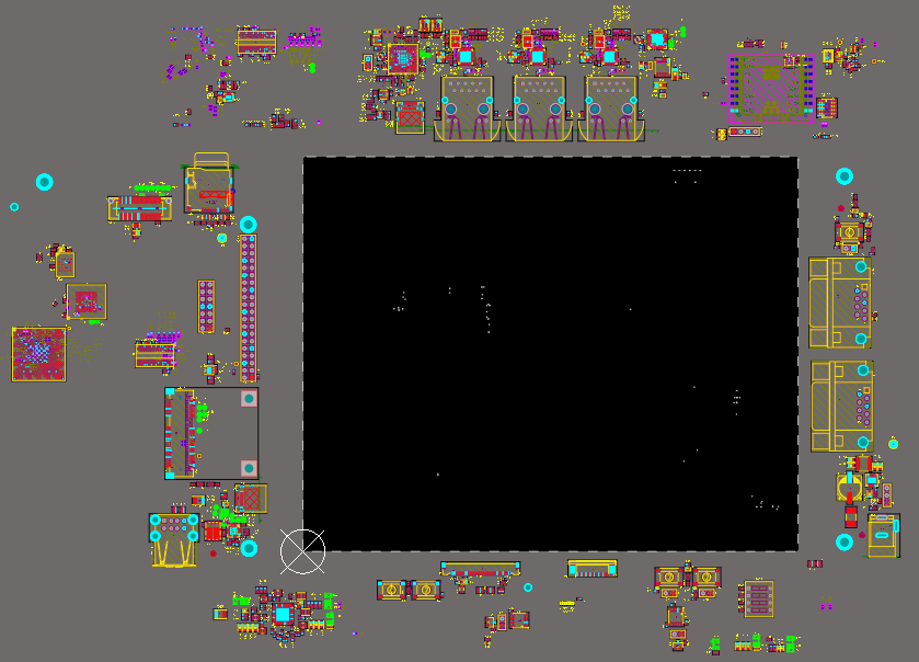
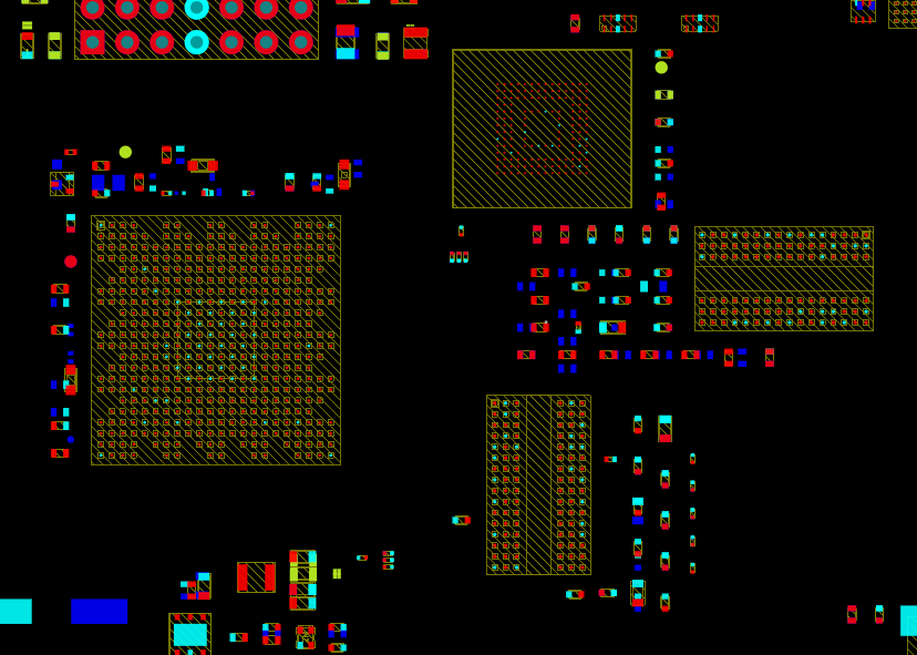
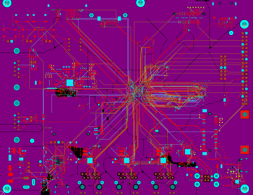
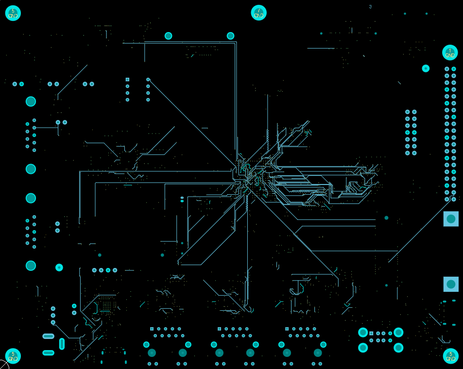
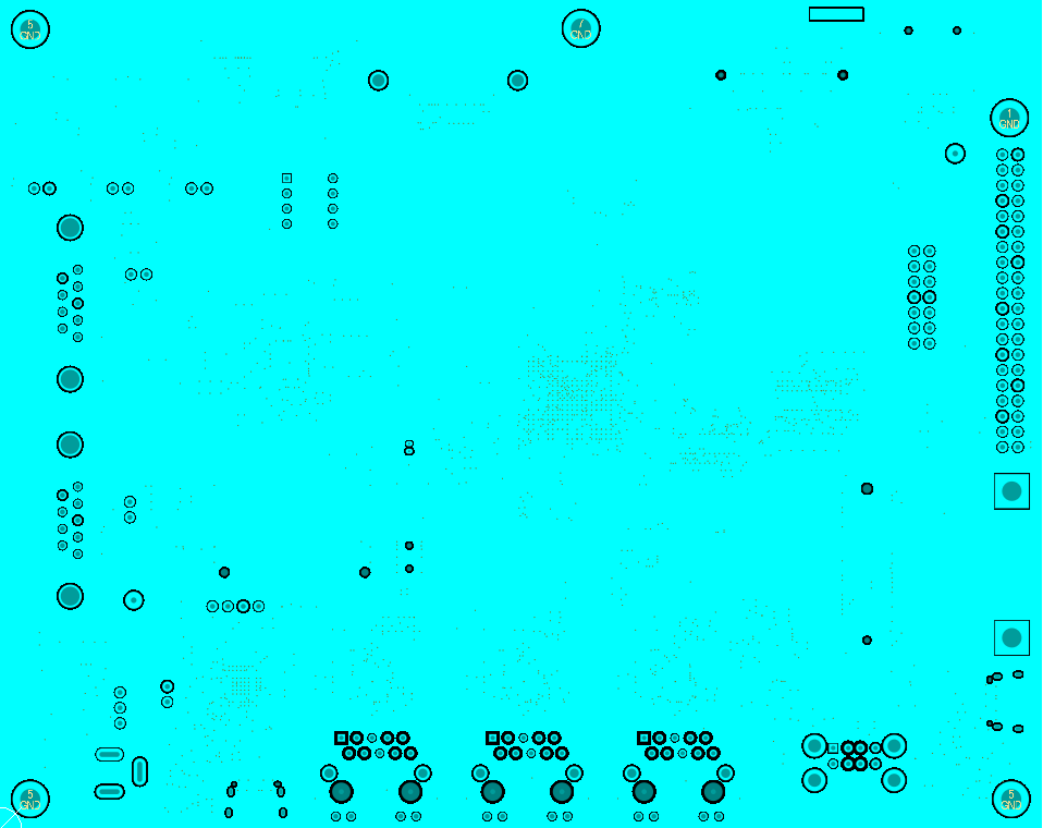
Placement Results
The automated placement positioned all components within the board outline while maintaining the functional groupings identified during schematic analysis. The following screenshots show the placement output from the tool.
Placement Comparison With Reference Design
The automated placement was compared against ST's original reference layout. While the exact positions differ (the automation makes its own grouping decisions), the functional clustering is similar — DDR4 components near the processor memory bus, PMIC components forming a compact power island, and interface connectors along the board edges.
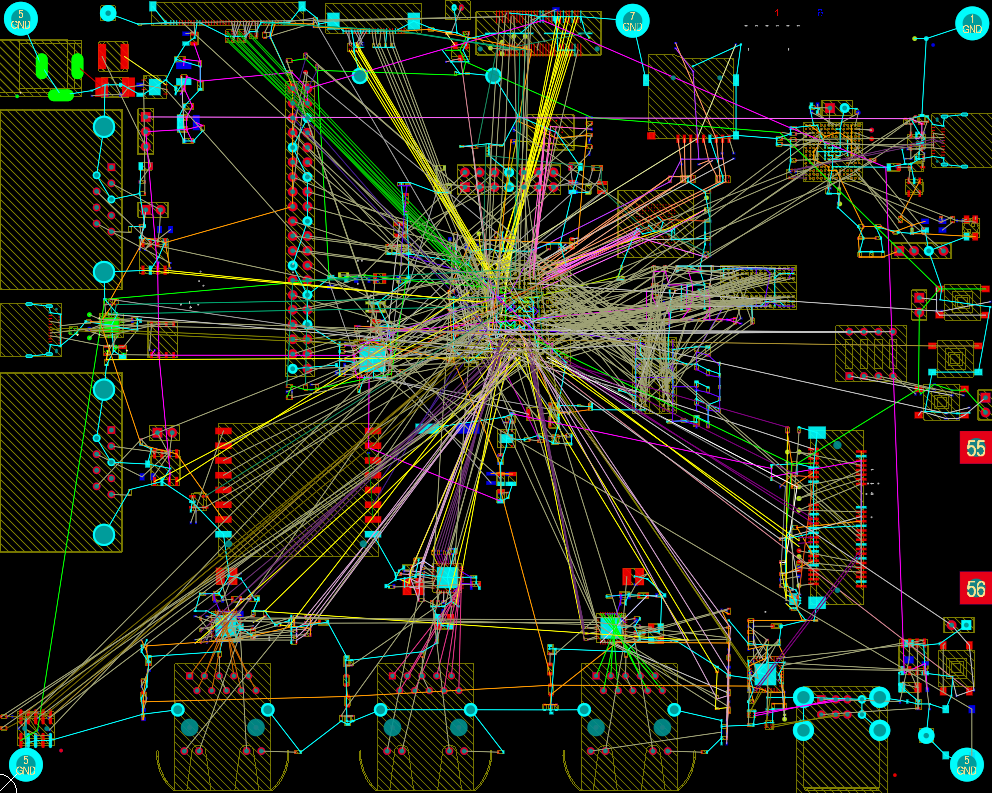
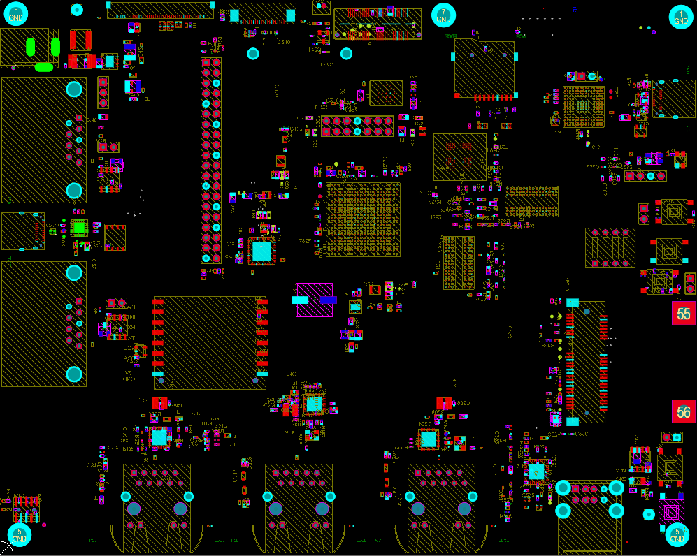
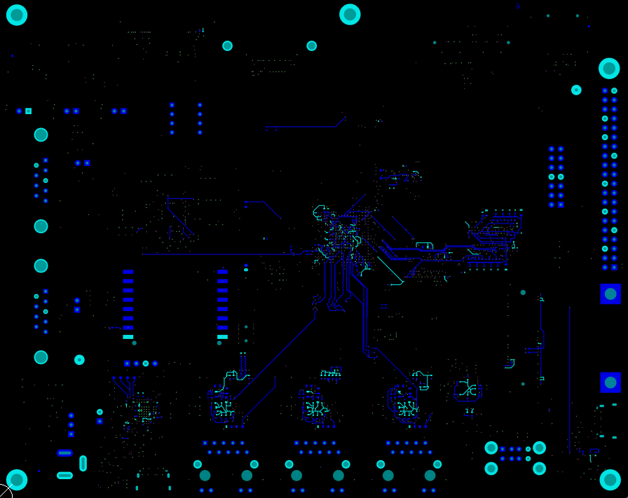
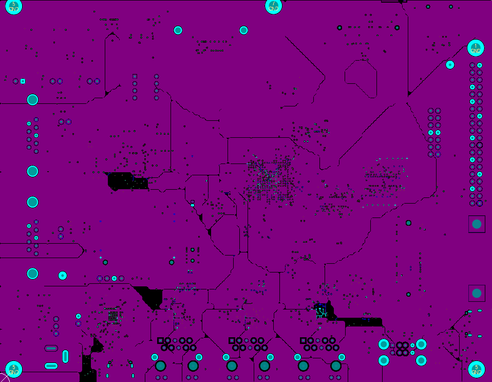
Routing Results
The routing engine completed all signal connections across the configured layer stackup. The following screenshots show the routing output before manual refinement.
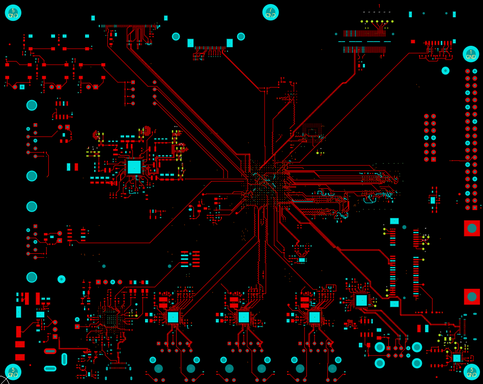
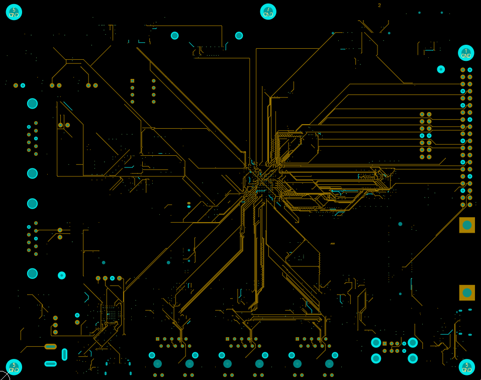
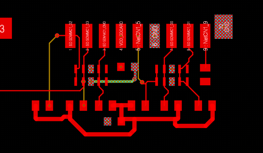
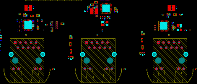
Differential Pair Routing
The board carries several differential pair groups across different interfaces, each with its own impedance and spacing requirements. The automation routed these pairs while maintaining the configured spacing rules. The following screenshots show the differential routing output.
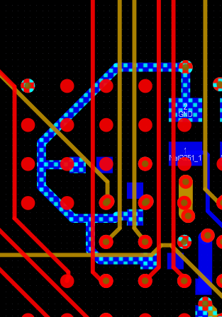
While the automation maintained pair spacing during routing, length matching precision and impedance tuning required manual verification. See the Manual Refinement section for details on what the engineer adjusted.
Key Highlights
Functional Block Grouping
The placement algorithm grouped the STM32MP257FAI3 with its DDR4 memory and decoupling network, the STPMIC25 and its associated inductors and feedback components as a compact power island, and each Ethernet PHY with its nearest connector. These groupings were derived directly from the schematic topology — no manual configuration of grouping rules was required.
BGA Fanout Routing
Escape routing from the TFBGA436 was handled in full by the automation — covering all 436 pins with via placement and layer transitions to open routing channels without clearance violations. Manually setting up fanout for a 436-pin fine-pitch BGA is a significant time investment that the automation handles directly.
Multi-Interface Differential Pair Routing
DDR4, three Gigabit Ethernet channels, and USB Type-C differential pairs were all routed in a single automated run with their configured spacing constraints applied. The automation handled pair routing across all interfaces simultaneously without the engineer manually sequencing each interface.
Priority-Based Routing Sequence
The routing engine ordered nets by signal criticality — power and return paths first, then differential pairs with impedance constraints, then general-purpose signals. This sequencing reduces the likelihood of critical nets being blocked by lower-priority routes in constrained routing channels.
DFA/DFM Report Generation
Alongside the routed board, the automation produced Design for Assembly and Design for Manufacturability reports as part of the same run, giving the engineer a structured review document without additional tooling.
Automation Strengths
The following capabilities were demonstrated on this board and are relevant to engineers considering automation for designs of similar complexity.
Schematic-Driven Placement — No Manual Net List Preparation
The automation read the Altium schematic directly to extract circuit topology, functional block structure, and net relationships. The engineer does not need to prepare a separate netlist or manually configure grouping rules before running placement.
Handles Interface Density Without Manual Routing Channel Setup
On a board where DDR4, triple Ethernet, USB, PCIe, and display interfaces all compete for routing channels, the automation allocated layer assignments and via strategies across all interfaces in a single pass. Managing this manually requires sequential decision-making that compounds in time as interface count increases.
IP Protection — Local Execution
Design automation runs on the engineer's local system. Design data does not leave the machine, which is relevant for development boards subject to IP or NDA constraints.
Minimal Configuration Setup
Beyond the design rules file and board outline, placement and routing decisions were derived from the schematic. Engineers configure constraints once and let the automation interpret the design intent rather than manually directing each routing decision.
What Required Manual Engineering
Automation does not replace the layout engineer. It handles the repetitive and time-consuming aspects of placement and routing, producing a starting point that an engineer then reviews and refines. Below is a breakdown of what the tool handled versus what required human judgment.
| Design Step | Automation | Engineer Review / Refinement |
|---|---|---|
| Schematic import and net classification | Handled by tool | — |
| Component grouping by functional block | Handled by tool | — |
| Component placement within board outline | Handled by tool | Crystal oscillator and sensitive analog circuit repositioning |
| Decoupling capacitor placement | Placed near power pins | Fine-tuning for specific PMIC output rails |
| General signal routing | Handled by tool | Some traces rerouted for cleaner layer transitions |
| Differential pair routing (DDR4, Ethernet, USB) | Initial routing with configured spacing | Length matching tuning, impedance verification, spacing adjustments |
| Power plane generation | Initial plane fills created | Plane splits and pour priority adjustments |
| Via optimization | Functional vias placed during routing | Redundant via removal, via stitching for ground continuity |
| DRC compliance | Basic DRC pass completed | Manufacturer-specific rule verification, remaining violation resolution |
Design Results Comparison
Traditional Manual Design
- Significant engineering time for TFBGA436 BGA fanout and differential routing at this interface density
- Multiple manual iteration cycles typical for boards with DDR4, triple Ethernet, and PCIe simultaneously
- Requires an experienced layout engineer with BGA escape discipline and high-speed interface knowledge
- Complete engineer control over all placement and routing decisions throughout
- Optimal results achievable with a skilled, experienced designer
- Manual verification of all clearances, length matching, and design rules
Automated Approach
- ~10 minutes for automated placement, ~5 hours for automated routing
- Manual refinement still required — particularly for DDR4 length matching, differential pair tuning, and power plane verification
- Reduces time spent on initial placement, BGA fanout setup, and multi-interface routing sequencing
- Schematic-driven — placement and routing decisions derived directly from circuit topology
- Integrated placement, routing, and DFA/DFM report generation in a single run
- Engineering review and refinement required before production use
Honest Assessment
This automation does not replace the layout engineer, particularly on a board with multiple high-speed interfaces, a 436-pin BGA, and a dedicated PMIC with complex power distribution. What it provides is a substantially complete starting point — component placement, BGA fanout, and signal routing across all interfaces — that an engineer reviews, adjusts, and refines rather than building from a blank board. Length matching for DDR4 and differential pair fine-tuning remain engineering tasks. Production readiness requires engineering judgment throughout.
Time Comparison
Understanding the Time Comparison
The 2.5-week estimate for manual design reflects the minimum effort expected from an experienced layout engineer working on a board of this complexity — a TFBGA436 processor with DDR4, triple Gigabit Ethernet, multiple display interfaces, and a dedicated PMIC, all within a constrained board outline. This estimate accounts for the additional high-speed interface fine-tuning this board demands: DDR4 intra-group length matching, differential pair impedance verification across three Ethernet channels and USB Type-C, and power plane iteration for the multi-rail PMIC. It covers placement, routing, DRC iteration, and design review cycles.
The automated output still requires engineer review and refinement time. The total end-to-end time with automation depends on how much refinement is needed for the specific project requirements. The automation compresses the initial placement and routing phase; it does not eliminate the need for engineering judgment.
Current Limitations
Transparency about what the tool cannot do is as important as showing what it can. The following limitations were observed during this case study.
Differential Pair Length Matching
While differential pairs were routed with configured spacing, precise length matching for DDR4 data groups and Ethernet TX/RX pairs required manual tuning. The automation does not yet perform fine-grained length equalization for timing-critical buses.
Via Count Optimization
The routing engine generates functionally correct connections but places more vias than an experienced designer would use. Reducing via count improves both signal quality and manufacturing yield. Manual consolidation was required in several areas.
Power Plane Refinement
Automated power plane fills required manual adjustment for proper split boundaries, pour priorities, and thermal relief tuning. The tool creates initial plane structures, but an engineer needs to verify current distribution and plane continuity.
Manufacturer-Specific DRC
Basic design rule compliance was achieved, but some fabrication house-specific rules (annular ring tolerances, solder mask expansion, specific via-in-pad requirements) needed manual verification against the target manufacturer's specification sheet.
Conclusion
The STM32MP257F-EV1 is a complex, real-world evaluation board with a 436-pin BGA processor, DDR4 memory, triple Gigabit Ethernet, and multiple mixed-signal interfaces. Automating its placement and routing demonstrates what current AI PCB automation in Altium can deliver — and where it still needs an engineer in the loop.
The tool placed all components in approximately 10 minutes and completed routing in approximately 5 hours. The automated output required engineer review for differential pair tuning, via optimization, and power plane refinement. These are areas where experienced layout engineers apply judgment that automation has not yet replicated fully.
This case study joins our KiCad automation case study in documenting what the tool does on real boards, with real constraints, using actual design files — including where the results fall short.
Want to Discuss This Case Study?
If you have questions about the results, the methodology, or how automation handles boards similar to yours, reach out to our engineering team.
Request a Technical Discussion